| Diameter |
4" |
5" |
6" |
8" |
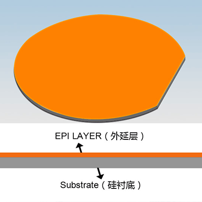
| Epitaxy Layer |
Dopant |
Boron, Phos, Arsenic |
| Orientation |
<100>, <111> |
| Conductivity type |
P/P++, N/N++, N/N+, N/N+/N++, N/P/P, P/N/N+ |
| Resistivity |
0.001-50 Ohm-cm |
| Res. Uniformity |
Standard <6%, Maximum Capabilities <2% |
| Thickness (um) |
0.1-150 |
| Thickness Uniformity |
Standard <3%, Maximum Capabilities <1% |
| Substrate |
Orientation |
<100>, <111> |
| Conductivity type / Dopant |
P Type/Boron , N Type/Phos, N Type/As, N Type/Sb |
| Thickness (um) |
300-725 |
| Resistivity |
0.001-100 Ohm-cm |
| Surface Finished |
P/P, P/E |
| Particle |
<50@0.5um |
Pluto provides a variety of production proven and industry standard Silicon Epitaxy process technologies for some of the most essential microelectronics applications:
Diodes
• Schottky diodes
• Ultra-fast diodes
• Zener diodes
• PIN diodes
• Transient Voltage Suppressors (TVS)
• and other
Transistors
• Power IGBT
• Power DMOS
• MOSFET
• Medium power
• Small-signal
• and other
Integrated Circuits
• Bipolar ICs
• EEPROM
• Amplifiers
• Microprocessors
• Microcontrollers
• RFID
• and other
To Integrated Circuit manufacturers PLUTO offers Silicon Epitaxial Deposition Services on substrates with buried ion-implanted or diffused layers.
Silicon substrates are either purchased from major global vendors or supplied by customer.
Epitaxy is a kind of interface between a thin film and a substrate. The term epitaxy (greek; "epi" "above" and "taxis" "in ordered manner") describes an ordered crystalline growth on a (single-) crystalline substrate. It involves the growth of crystals of one material on the crystal face of another (heteroepitaxy) or the same (homoepitaxy) material. The lattice structure and orientation or lattice symmetry of the thin film material is identical to that of the substrate on which it is deposited. Most importantly, if the substrate is a single crystal, then the thin film will also be a single crystal. Contrast with self-assembled monolayer and mesotaxy.
Some examples are molecular beam epitaxy, liquid phase epitaxy and vapor phase epitaxy. It has applications in nanotechnology and in the manufacture of semiconductor and photonic devices. Indeed, epitaxy is the only affordable method of high crystalline quality growth for many semiconductor materials, including the technologically important materials as SiGe, gallium nitride, gallium arsenide and indium phosphide, the latter used in devices for LEDs and telecommunications.
Epitaxial-growth means the crystal growth being conducted on crystal of substrate and disposed in accordance with foundation of substrate crystal phase.
Homoepitaxial means the growth of the same material as the substrate while heteroepitaxial means the growth of the different material from the substrate. Substrate wafer on which single crystal thin film deposited by epitaxial growth are generally called as epi wafer.
Silicon epi wafers are utilized for element of diode and transistor or substrate for IC such as bipolar type and MOS type.
Furthermore, multiple layer epi wafers and thick film epi wafers are often used for power device and contribute to smallness and energy-saving of various power-source products.
PLUTO can provide epitaxial grade wafers from our inventory or can grow custom epitaxial layers to meet your exact specifications.
Please CONTACT PLUTO for further information on epitaxial grade wafers (EPI), to request or to discuss your current requirements or visit our ONLINE INVENTORY.