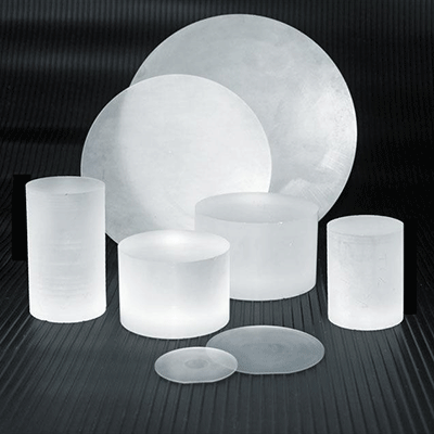
In general, the epitaxial layer of gan-based materials and devices is mainly grown on the sapphire substrate. Sapphire substrate has many advantages: first, sapphire substrate production technology mature, device quality is better; Secondly, sapphire has good stability and can be used in the process of high temperature growth. Finally, sapphire has high mechanical strength and is easy to handle and clean. Therefore, most processes generally use sapphire as a substrate.
There are also some problems with using sapphire as a substrate, such as lattice mismatch and thermal stress mismatch, which can cause a lot of defects in the epitaxial layer and make subsequent device processing difficult. Sapphire is a kind of insulator, room temperature resistivity of more than 1011 Ω · cm, in this case cannot make vertical structure of the device; N - and p-type electrodes are usually made only on the outer surface of the epitaxial layer. The fabrication of two electrodes on the upper surface reduces the effective luminous area and increases the lithography and etching processes in device manufacturing, resulting in lower material utilization and higher cost. Due to the difficulty of p-type GaN doping, the method of preparing metal transparent electrode on p-type GaN is widely used to diffuse the current and achieve the goal of uniform luminescence. However, the metal transparent electrode generally absorbs about 30% to 40% of the light. Meanwhile, gan-based materials have stable chemical properties and high mechanical strength, so it is not easy to etch them. Therefore, better equipment is needed in the etching process, which will increase the production cost.
Sapphire is very hard, second only to diamond in hardness among natural materials, but it needs to be thined and cut (from 400 m to about 100 m) during the manufacture of LED devices. The acquisition of equipment to complete the thinning and cutting process will require a major increase in investment.
The thermal conductivity of sapphire is not very good (about 25W/ (m·K) at 100℃). Therefore, when using LED devices, a lot of heat will be transferred; Thermal conductivity is a very important factor especially for large power devices. In order to overcome the above difficulties, many people try to grow GaN photoelectric devices directly on the silicon substrate, so as to improve the thermal and electrical conductivity.


