| GaN/ Al2O3 Substrates (4") | |||
| Item | Un-doped | N-type | High-doped N-type |
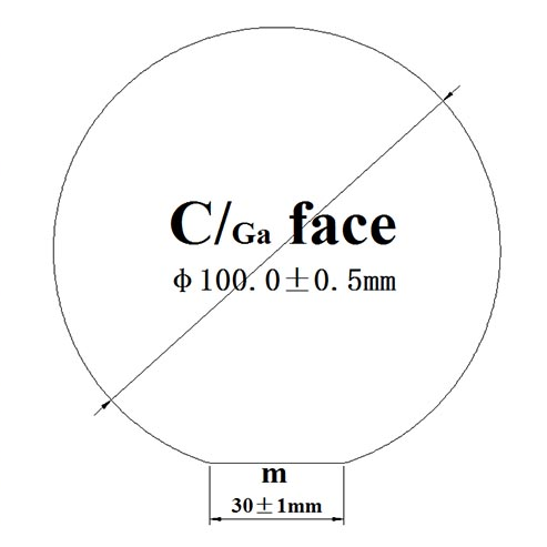
| Size (mm) | Φ100.0±0.5 (4") | ||
| Substrate Structure | GaN on Sapphire(0001) | ||
| SurfaceFinished | (Standard: SSP Option: DSP) | ||
| Thickness (μm) | 4.5±0.5; 20±2;Customized | ||
| Conduction Type | Un-doped | N-type | High-doped N-type |
| Resistivity (Ω·cm)(300K) | ≤0.5 | ≤0.05 | ≤0.01 |
| GaN Thickness Uniformity | ≤±10% (4") | ||
| Dislocation Density (cm-2) | ≤5×10⁸ | ||
| Useable Surface Area | >90% | ||
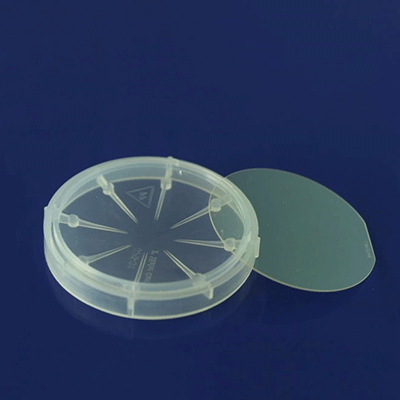
| Package | Packaged in a class 100 clean room environment. | ||