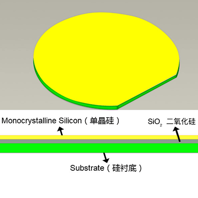
In order to improve the integration and speed of integrated circuits, the size of devices must be reduced to reduce the power consumption. However, when the size of the device is reduced to the submicron range, the conventional structure is not suitable, which leads to the development of SOI (silicon on insulator or semiconductor on insulator) structure, that is, the device is made on the silicon single crystal layer grown on the insulating substrate. SOI structure was proposed for submicron CMOS devices to replace the conventional structure which is not suitable for the requirements and the applied SOS structure (SOS can be regarded as a form of SOI). However, SOI structure soon became a new way to realize high-speed integrated circuit and three-dimensional integrated circuit (but not all SOI structures can be used for three-dimensional integrated circuit), which is a current semiconductor material research hotspot issues.