Thin Film Deposition
Various thin films in semiconductor devices are fundamental to chip functionality. Thin film deposition refers to the process of depositing metals, non-metals, or compound materials onto a substrate surface in the form of atoms/molecules under vacuum or gas‑phase environments, forming dense, uniform, and thickness‑controllable solid films. As a core step in semiconductor manufacturing, the quality of deposited films directly determines the electrical performance, reliability, and yield of devices.
Our company (PlutoSemi) offers a thin film deposition platform covering two major technology routes: Physical Vapor Deposition (PVD) and Chemical Vapor Deposition (CVD). Equipped with multiple advanced deposition tools, we meet thickness requirements from nanometers to micrometers, and support various substrate materials including silicon, compound semiconductors, glass, sapphire, and flexible substrates.
I. Technology Principles
Physical Vapor Deposition (PVD): Under vacuum, source material atoms are ejected by heating or sputtering and deposited onto the substrate. Methods include electron beam evaporation, magnetron sputtering, and ion beam sputtering.
Chemical Vapor Deposition (CVD): Gaseous precursors react on the substrate surface to form solid films. Methods include LPCVD, PECVD, and atomic layer deposition (ALD).
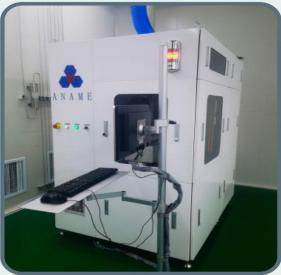
II. Equipment and Process Capabilities
Our thin film deposition platform includes the following key equipment:
|
Process Category |
Equipment Model |
Representative Deposited Materials |
| Electron Beam Evaporation (EBE) |
Ohmiker‑50B, Fu‑12PEB |
Ti, Al, Ni, Au, AuGe, Cr, Pt, In, Sn and other metals/alloys |
| Magnetron Sputtering (PVD) |
MSP‑3200E, JCPY600, orion8 |
Ti, Al, Ni, Au, Ag, Cr, Pt, Cu, TiW90, Pd, Zn, Mo, W, Ta, Nb, ITO, and various compounds |
| Ion Beam Sputtering (IBS) |
Discovery HDG |
Dense metal/oxide films, also with etching capability |
| Optical Coating |
OTFC‑900DBI |
IR cut filters, dichroic filters, other optical thin films |
| PECVD |
PlasmaPro 800Plus |
SiO₂, SiNx dielectric layers, passivation layers |
| LPCVD |
TYTAN 4600 / TYTAN 3600 |
SiO₂, Si₃N₄, polysilicon |
| ALD |
R200‑Adv, ELEGANT II‑200 |
Al₂O₃, TiO₂, HfO₂, AlN, TiN, Si₃N₄, Pt, etc. |
III. Material & Substrate
Material
Magnetron sputtering: Ti, Al, Ni, Au, Ag, Cr, Pt, Cu, TiW90, Pd, Zn, Mo, W, Ta, Nb, etc.
Electron beam evaporation: Ti, Al, Ni, Au, AuGe, Cr, Pt, In, Sn, etc.
Chemical deposition: SiO2, SiNx, a-Si
Substrate
Silicon wafers, quartz glass wafers, sapphire wafers, PET, Pi, etc.