Lithography
Process introduction
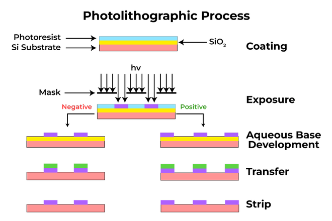
Lithography is an important step in the semiconductor device manufacturing process, using exposure and development on the photoresist layer to depict the structure of the device, and then through the etching process to convert the graphics on the mask to the substrate. MEMS currently master electron beam lithography, step lithography, contact lithography and other lithography technologies
Technical application
Lithography is mainly used in semiconductor devices, integrated circuit manufacturing process.
Application materials
Wafers, glass, sapphire, flexible materials, etc.
Process capability
Step lithography: stepper i7/i1 0/i12, minimum line width 600nm, alignment deviation accuracy ±200nm
Contact and proximity lithography: MA6/BA6 lithography machine, minimum line width 2um, exposure error ±0.5um
Ultraviolet lithography, duplex lithography, alignment engraving
Size: 8', 6', 4', 2'