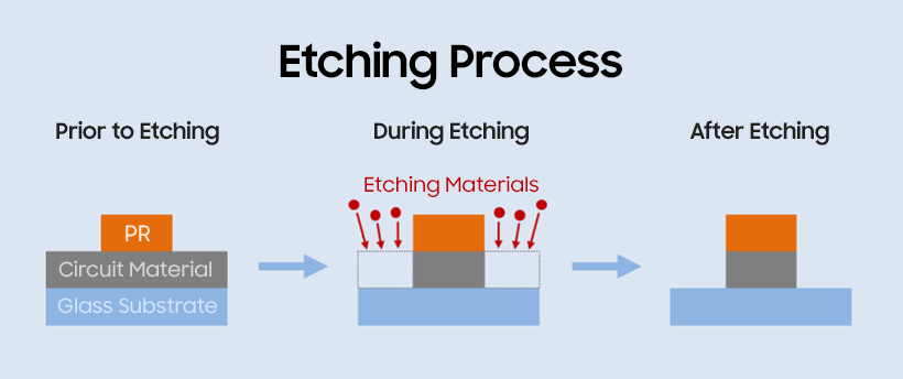
Etching is the technique of selective etching of a semiconductor substrate surface or surface coverage film according to a mask pattern or design requirement, and is a fairly important step in the semiconductor manufacturing process, microelectronic IC manufacturing process and micro-nano manufacturing process. It is a major process of patterned (pattern) processing associated with photolithography. Etching is divided into dry etching and wet etching. At present, Pluto has mastered a variety of etching processes, and will design etching solutions with good etching effect and high cost performance according to customers' needs.
Technical application
Etching technology is used in semiconductor devices, integrated circuit manufacturing, thin film circuits, printed circuits and other micrographics processing.
Process capability
Deep Silicon Etching (DRIE): wafers 8 inches and below, depth-to-width ratio 5:1
Ion Beam etching (IBE): Metal etching, 6 inches and below
Reactive ion etching (RIE), inductively coupled (ICP) plasma etching
Etching material
Silicon, silicon oxide, silicon nitride, metal, quartz and other materials