Doping
Doping is the process of introducing a small amount of specific impurity atoms into a pure semiconductor material to control the concentration and type of charge carriers, thereby modifying its electrical properties.
Types of Doping
N‑type doping: Adding pentavalent elements (e.g., phosphorus, arsenic) to a tetravalent semiconductor. This creates free electrons, and conduction depends on electrons (Negative).
P‑type doping: Adding trivalent elements (e.g., boron) to a tetravalent semiconductor. This creates holes, and conduction depends on holes (Positive).
The combination of N‑type and P‑type semiconductors forms the basis of the PN junction, which is the core logic for current control in chips.
Classification of Doping Techniques
Diffusion Doping – High-temperature thermal diffusion, low cost but poor precision.
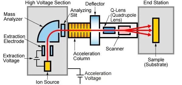
Ion Implantation Doping – High-energy ion bombardment with annealing, high precision and ultra‑shallow junctions.
PlutoSemi Ion Implantation Services
Process introduction
Ion implantation, gas source doping, and solid source doping are the main methods used to manufacture doped silicon in semiconductor devices.
Technical application
Metal finishing and materials science research.
Process capability
Injection materials: B, P, F, Al, N, Ar, Mg, Si and other elements
Injection angle: ±11°
Wafer size: compatible with 6 inches or less
Supporting processes: High‑temperature oxidation, high‑temperature diffusion, rapid annealing