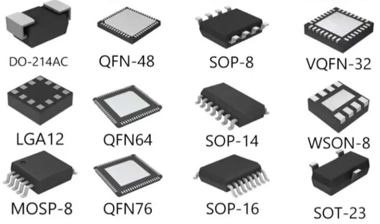
Packaging
Packaging Technology
Packaging is the final step in the micro‑nano manufacturing process, designed to protect fabricated micro‑nano devices. The packaging process must ensure that devices are safeguarded against damage during transportation, handling, and actual use, while maintaining their performance stability. Modern packaging technologies must consider not only physical protection but also thermal management, electrical interconnection, and other critical factors.
Wafer‑Level Packaging (WLP)
Wafer‑level packaging is a process performed directly on the completed wafer without singulating and packaging each chip individually. It mainly includes two types:
Wafer‑Level Chip Scale Packaging (WLCSP)
Wafer‑Level Integrated Packaging (WLIP), which further covers multi‑layer structures and System‑in‑Package (SiP)
Key Advantages
Miniaturization: Packaging is done directly on the wafer, reducing the excess volume of traditional packaging and enabling chip miniaturization.
High Performance: Circuits are interconnected directly during packaging, shortening signal paths, reducing latency, and improving performance.
High Integration: Supports integration of multiple chips and heterogeneous materials, suitable for multi‑function electronic products.
Cost Reduction: The process is completed in one batch on the wafer, eliminating singulation and individual packaging, simplifying the workflow and increasing production efficiency.
Typical Application Areas
Mobile & Consumer Electronics – Miniaturization, efficient heat dissipation
IoT Devices – Integration of communication, sensing, storage, processing
Automotive Electronics – High reliability for ADAS, onboard sensors
5G Equipment – High frequency, low latency
Future Trends
Heterogeneous Integration – SiP for memory, logic, sensors, power
3D Packaging & Stacking – Higher density and performance
Adaptive Thermal Materials – Advanced heat dissipation
AI‑Driven Optimization – Improved yield and throughput