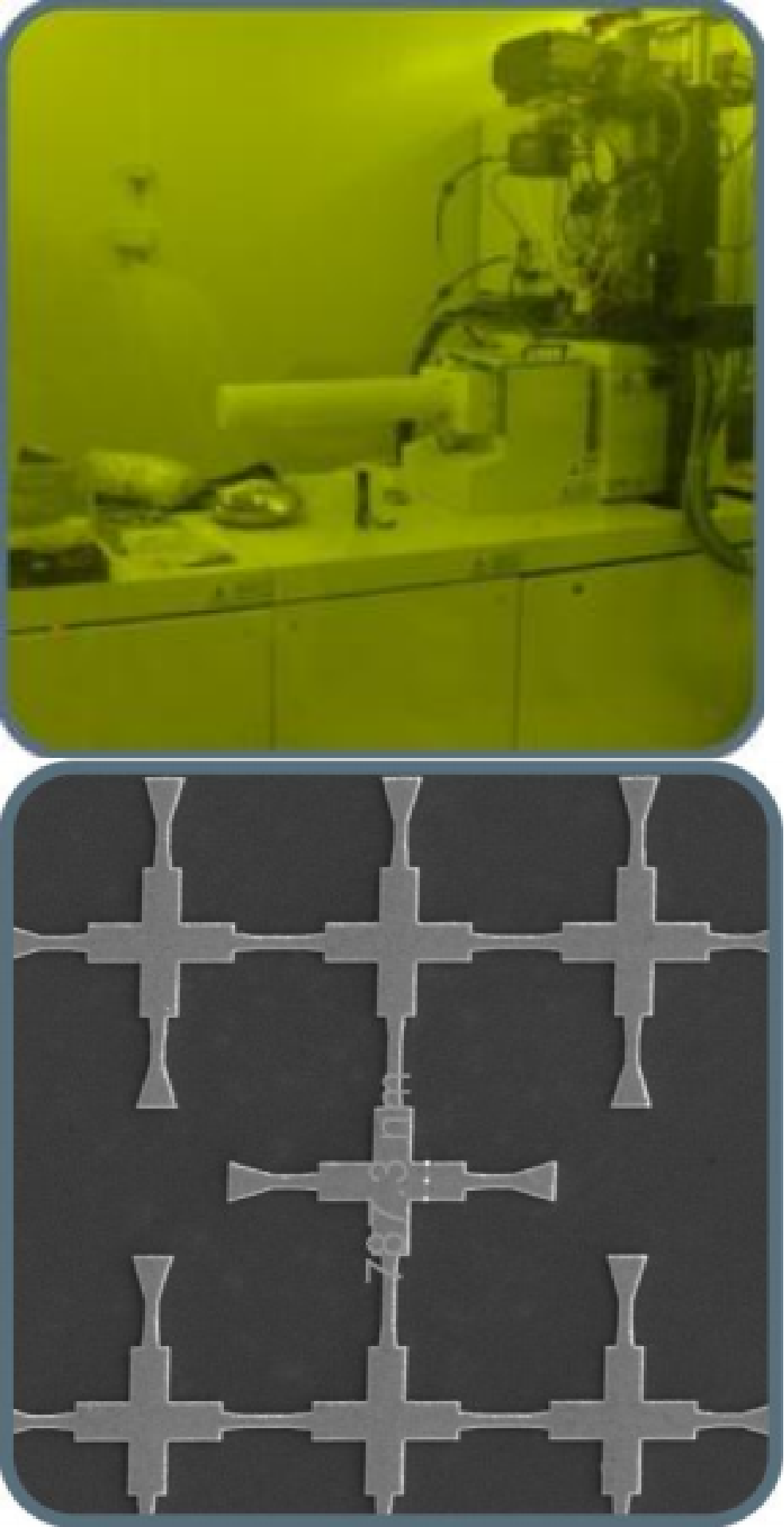
Electron Beam Lithography (EBL)
Model: VISTEC EBPG 5000 plus
Manufacturer: VISTEC LITHOGRAPHY, Netherlands
Main Functions: High-precision mask making, nano-patterning, nano-imprint template production, and various other needs for generating nano-level precision patterns.
Technical Specifications: Acceleration Voltage: 50kV~100kV
Minimum Electron Beam Spot Size: 2.2nm
Processing Accuracy: <8nm lines
Stitching Accuracy: <20nm @ 250 microns writing field @ 100kV
Writing Field Size: 256 × 256 microns @ 100kV, 409 × 409 microns @ 50kV
Electron Beam Current: 0.1nA to 100nA
Direct Write Wafer Sizes: 2 inch, 3 inch, 4 inch, 50mm, 100mm, 150mm (expandable),
Non-standard small wafers
Substrate Materials: Various solid substrate materials with smooth surfaces.