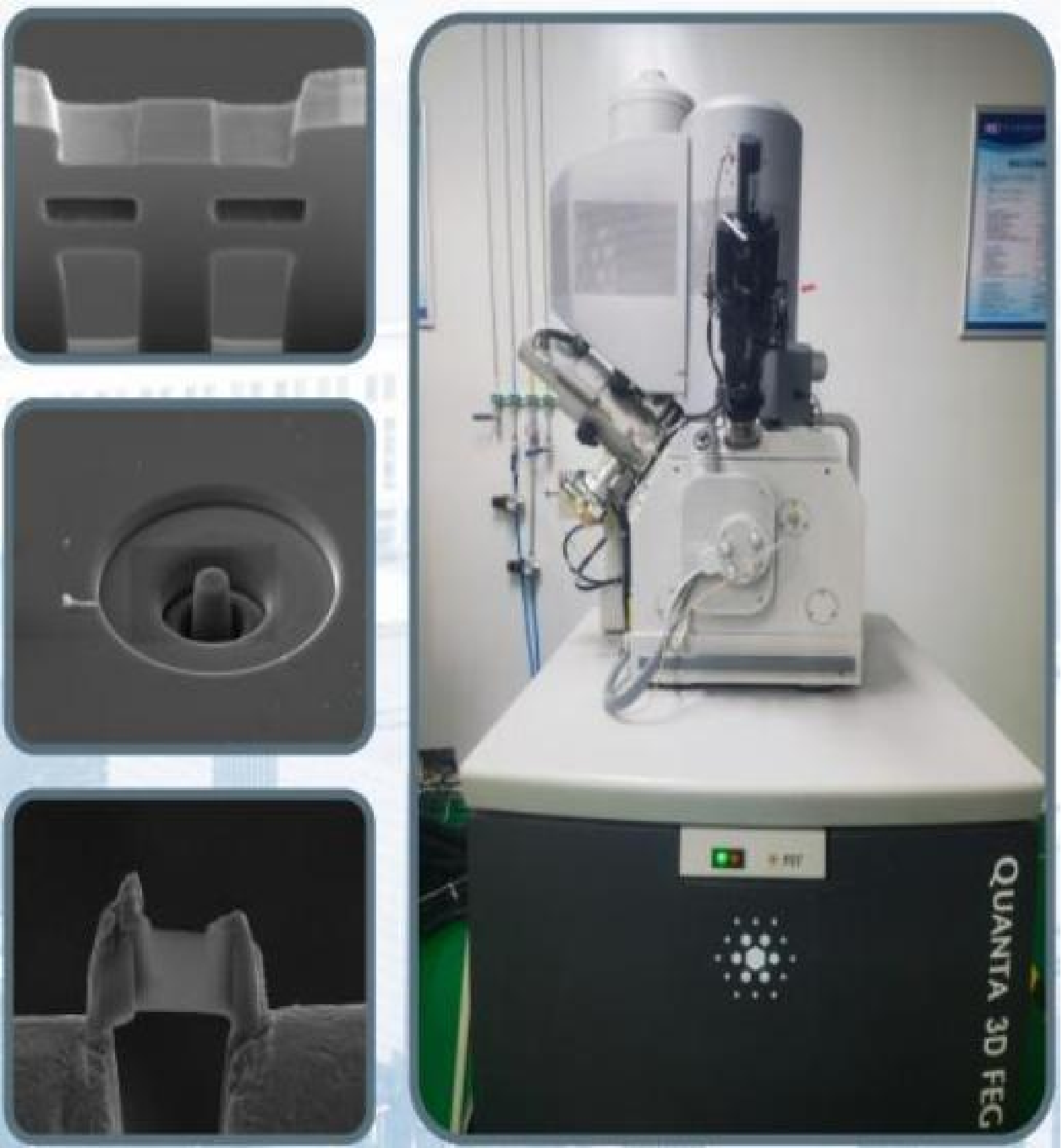
Electron Beam and Ion Beam Dual Beam System
Model: Quanta 3D FEG SEM/FIB
Manufacturer: FEI Company, USA
Main Function: The SEM/FIB dual beam system is primarily used for preparing micro-nano structures on solid samples such as metals, semiconductors, dielectrics, and multilayer film structures. Additionally, with the integration of a nano manipulator, it can prepare TEM samples at specific points. This instrument is a powerful tool for exploring the microscopic nature of the apparent properties of materials.
Technical Specifications: FIB maximum beam current reaches 65nA
Scanning electron microscope maximum electron beam current 200nA
Environmental scanning (ESEM) technology: three vacuum modes: high vacuum, low vacuum, and environmental vacuum:
1kV resolution (high vacuum) 2.9nm
3kV resolution (low vacuum) 2.9nm
30kV STEM (high vacuum) resolution 0.8nm