
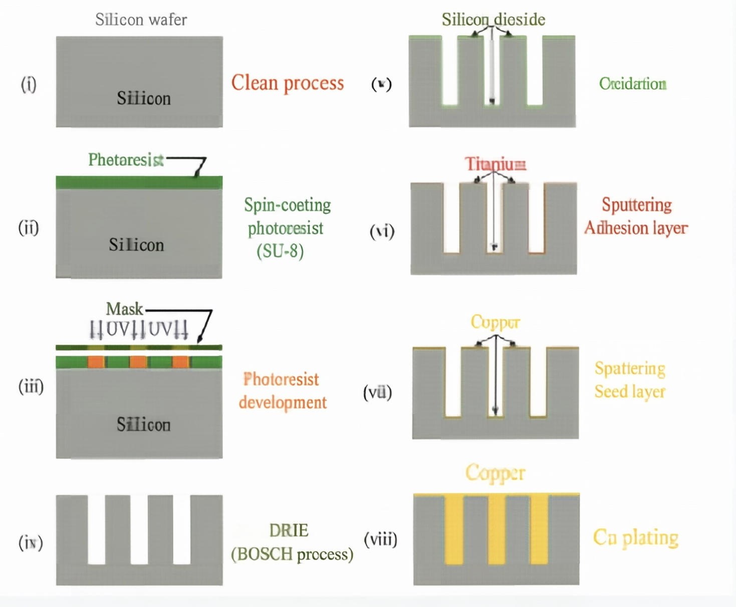
TSV
Through-Silicon Via (TSV) enables vertical chip stacking for higher bandwidth, lower power, and smaller form factors. Essential for HBM, 3D ICs, and AI accelerators.
|
Key Indicator |
Typical Parameter Range |
Remarks |
|
Aspect Ratio |
10:1 ~ 50:1 |
Advanced processes can reach 50:1 or higher; high aspect ratio facilitates pitch scaling. |
|
Via Diameter |
0.5µm~ 200µm |
Depends on application: Memory (small) vs. Power devices (large). |
|
Pitch |
5µm ~ 100µm |
Determines interconnect density; high-end logic chips pursue smaller pitches. |
|
Depth |
10µm ~ 200µm |
Depends on the final thickness after wafer thinning. |
|
Filling Material |
Copper, Tungsten, Polysilicon |
Copper is most common (good conductivity); Polysilicon is used for MEMS/partial CIS. |
|
Insulation Layer |
Silicon Dioxide, Silicon Nitride |
Must be dense and pinhole-free to prevent leakage. |
|
Barrier/Seed Layer |
Ti/TiN, Ta/TaN |
Prevents copper diffusion into the silicon substrate and ensures adhesion. |

