
|
Key Indicator |
Parameter Range |
Remarks |
|
Aspect Ratio |
10:1 ~ 50:1 (Up to 100:1 in labs) |
Glass processing is harder than silicon, but advanced laser processes have improved this significantly. |
|
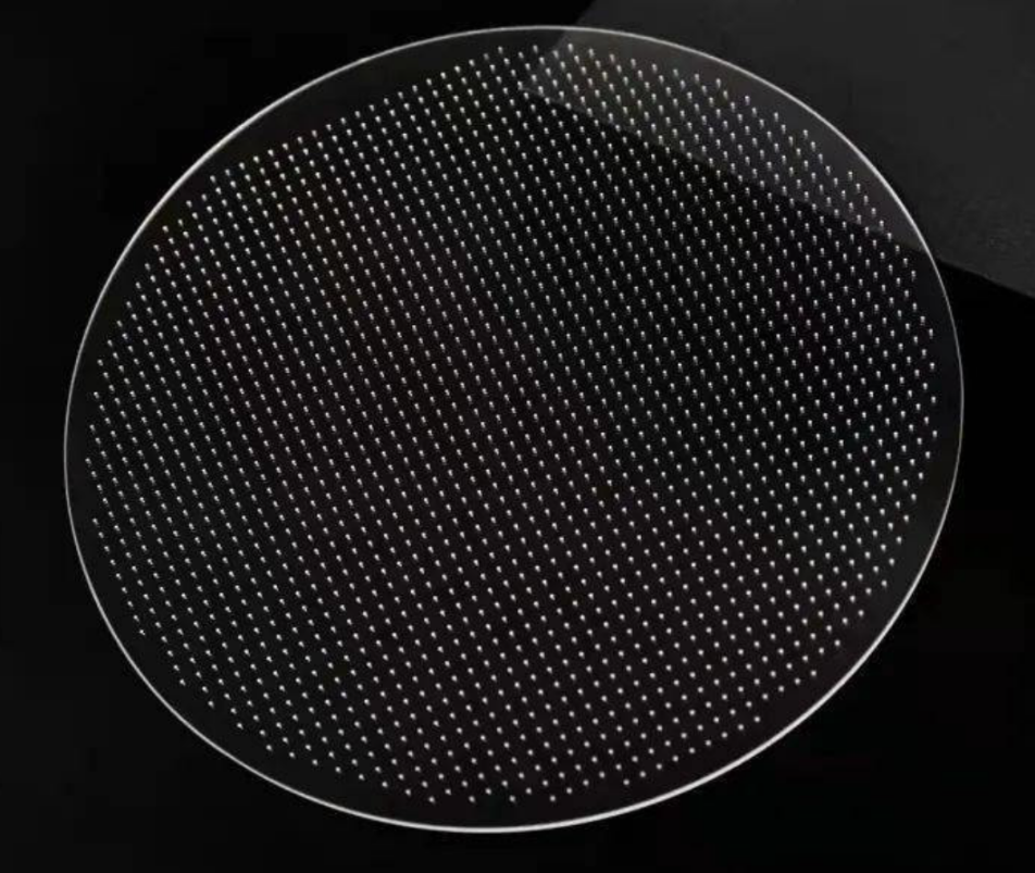
Via Diameter |
5µm ~ 100µm |
Glass is brittle; small vias require high-precision laser or etching. |
|
Glass Thickness |
50µm ~ 1100µm |
Common thickness is 100µm-500µm; ultra-thin glass processing is a trend. |
|
Dielectric Loss |
Very Low (tan δ ≈ 0.001) |
Glass has much lower RF loss than silicon, ideal for 5G/6G applications. |
|
Parasitic Capacitance |
Low |
No extra dielectric layer needed; direct metallization results in lower capacitance. |
|
Resistance |
< 10 mΩ |
Uses copper electroplating like TSV, offering excellent conductivity. |
|
Substrate Material |
Quartz, Borosilicate, Ultra-thin Glass |
Coefficient of Thermal Expansion (CTE) matching is critical to prevent cracking. |
|
Via Formation |
Ultrasonic Drilling, Laser Etching, Photo-structurable Glass |
Photo-structurable glass (e.g., Foturan) allows semiconductor-like photolithography. |
|
Metallization |
Seed Layer Sputtering + Cu Plating |
Key challenge is uniform seed layer coverage on deep hole sidewalls. |

