III-V compound semiconductor process line
Process and Equipment
● Lithography System: Nikoni9 stepper (line width ≤ 500nm), Vistec EBPG electron beam lithography (≤ 10nm)
● Epitaxy Equipment: MOCVD
● Etching Equipment: Oxford Instruments PlasmaPro 100 ICP etcher (GaN etching selectivity > 50:1)
● Packaging Equipment: Dicing saw, wire bonder, for connecting chips to peripheral circuits.
Service Item
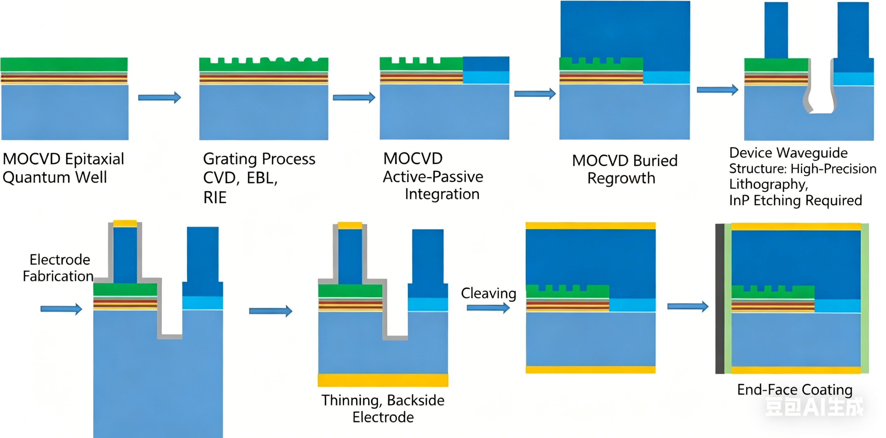
GaN HEMT device development, DFB laser process development
Process development and optimization
Failure analysis
Joint R&D:
Small-scale trial and pilot platform: providing "from epitaxy to packaging" full-process verification services for startups
Typical preparation devices
GaN Power Devices
28GHz, output power > 10W/mm
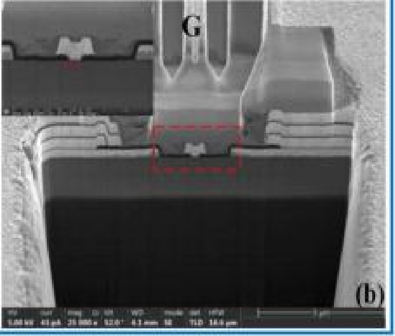
DFB Laser
Wavelength 1550nm, Output Power > 20mW
Microwave RF Switch
0.1-40GHz, Insertion Loss < 0.5dB
InGaAs infrared detector
wavelength 1.0-1.7 μm, dark current < 1 nA