Thin film lithium niobate process line
Process and Equipment
● Lithography System: Raith EBPG5000+ Electron Beam Lithography System (7nm linewidth
accuracy)
● Etching Equipment: ULVAC NLD Lithium Niobate Etching Machine
● Thin Film Equipment: Optical Coating Machine (Film Thickness Uniformity ±1.5%)
Service Item
Custom development of high-speed electro-optic modulators (bandwidth > 100GHz)
Quantum optical chips (entanglement sources/single-photon detectors) process
verification
Development of silicon photonic-lithium niobate heterogeneous integration
technology
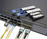
Core device foundry for data center optical modules (100G/400G PAM4 modulators)
Small batch wafer fabrication of microwave photonic devices
Typical preparation devices
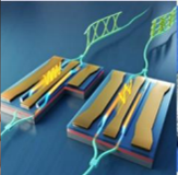
Ultra-fast Electro-Optic Modulator
3dB bandwidth > 110GHz, drive
voltage < 2V
Quantum Entangled Light Source
Entangled photon pair yield >
1MHz, purity > 98%
Optical Frequency Comb
delay accuracy < 1