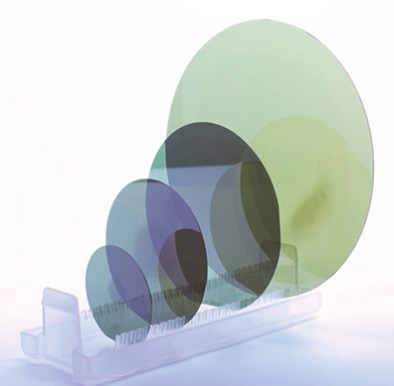
| Grade |
Zero MPD |
Production |
Research Grade |
Dummy Grade |
| |
Diameter |
100.0 mm±0.5 mm |
| |
Thickness |
4H-N |
350 μm±25μm |
| 4H-SI |
500 μm±25μm |
| |
Wafer Orientation |
Off axis : 4.0° toward < 1120 >±0.5° for 4H-N |
On axis : <0001>±0.5° for 4H-SI |
| |
Micropipe Density |
≤1 cm-2 |
≤5 cm-2 |
≤15 cm-2 |
≤50 cm-2 |
| |
Resistivity |
4H-N |
0.015~0.028 Ω·cm |
| 4H-SI |
≥1E5 Ω·cm |
| |
Primary Flat |
{10-10}±5.0° |
| Primary FlatLength |
32.5 mm±2.0 mm |
| Secondary FlatLength |
18.0mm±2.0 mm |
| Secondary FlatOrientation |
Silicon face up: 90° CW. from Prime flat ±5.0° |
| |
Edge exclusion |
3 mm |
| TTV/Bow /Warp |
≤15μm /≤25μm /≤40μm |
| |
Roughness |
Polish Ra≤1 nm |
| CMP Ra≤0.5 nm |
| Cracks by high intensity light |
None |
1 allowed, ≤2 mm |
Cumulative length≤10mm, single length≤2mm |
| Hex Plates by high intensitylight |
Cumulative area ≤1% |
Cumulative area ≤1% |
Cumulative area ≤3% |
| Polytype Areas by high intensity light |
None |
Cumulative area ≤2% |
Cumulative area ≤5% |
| Scratches by high intensity light |
3 scratches to 1×wafer diameter cumulative length |
5 scratches to 1×wafer diameter cumulative length |
5 scratches to 1×wafer diameter cumulative length |
| Edge chip |
None |
3 allowed, ≤0.5 mm each |
5 allowed, ≤1 mm each |
| Contamination by high intensity light |
None |
| |
|
|
|
|
|
|
|

