| Material | Applications |
| Silicon (Si) | Integrated circuits, MEMS, sensor substrates |
| Silicon Oxide (SiO₂) | Dielectric layers, optical waveguides, sacrificial layers |
| Silicon Nitride (Si₃N₄) | Passivation layers, waveguide cores, stress engineering layers |
| Material | Applications | Etching Challenges |
| Indium Phosphide (InP) | Lasers, photodetectors | Damage-sensitive, needs low-damage processes |
| Gallium Nitride (GaN) | HEMTs, power devices, LEDs | Chemically inert, needs high-bias physical assist |
| Sapphire (Al₂O₃) | LED substrates, RF front-ends | Hard material, slow etch rates |
| Material | Applications | Etching Key Points |
| Lithium Niobate (LiNbO₃) | Modulators, waveguides, SAW filters | Damage-sensitive, needs optimized gas chemistry |
| Lithium Tantalate (LiTaO₃) | RF filters (SAW/BAW) | Etch rate control is critical |
| Quartz (Crystalline SiO₂) | Optical communication devices, MEMS | Sidewall smoothness is key |
| Material | Applications |
| Titanium Oxide (TiO₂) | Anti-reflection layers, high-index waveguides |
| Tantalum Nitride (TaN) | Thin-film resistors, diffusion barrier layers |
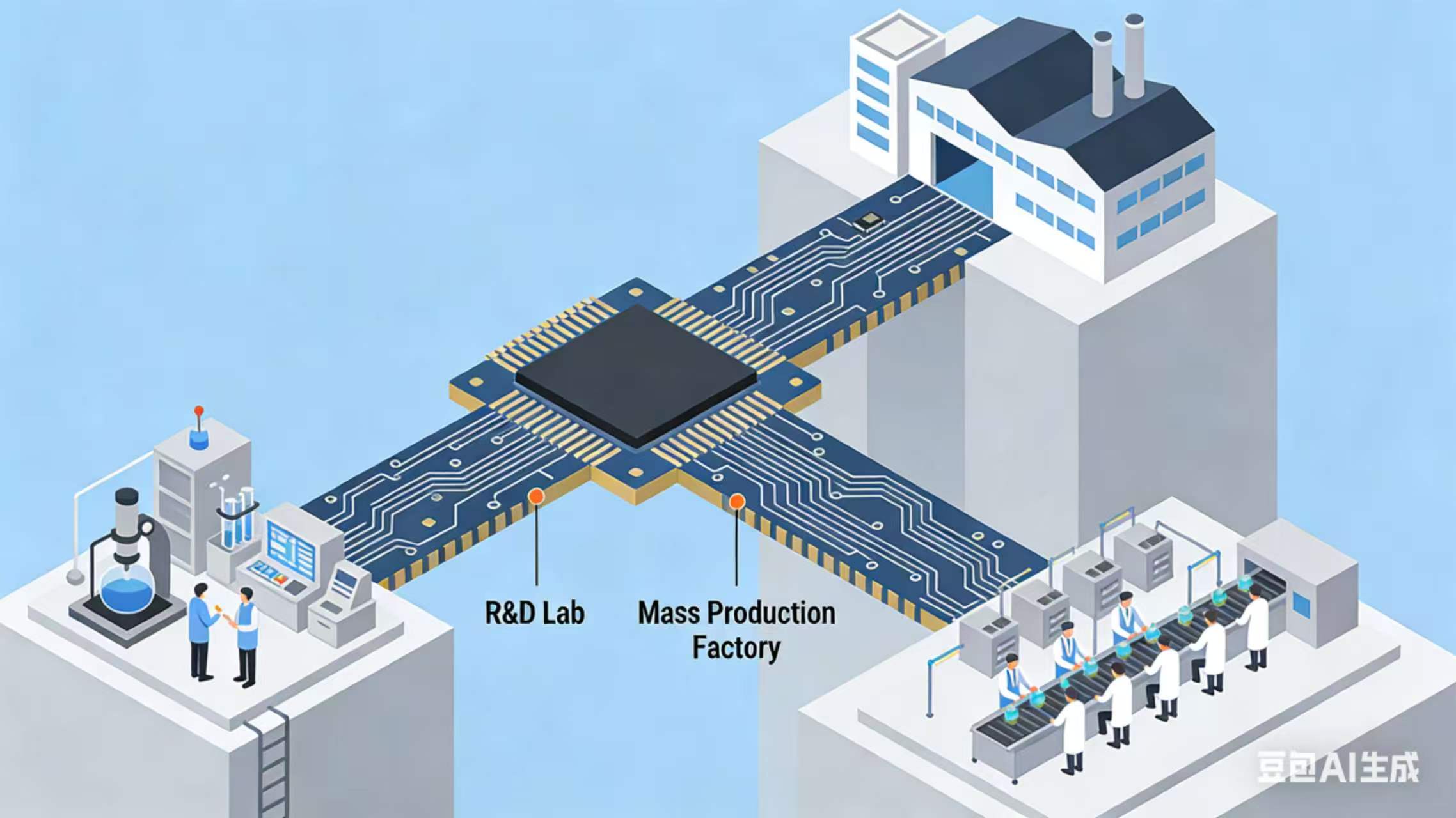
Different materials need different tools. We've got six types of etchers covering everything—from dielectrics to metals, from deep trenches to release etching.
| Equipment Type | Process | Specialty | Key Features |
| RIE | Reactive Ion Etching | Conventional dielectrics (SiO₂/Si₃N₄) | Stable, reliable, cost-effective |
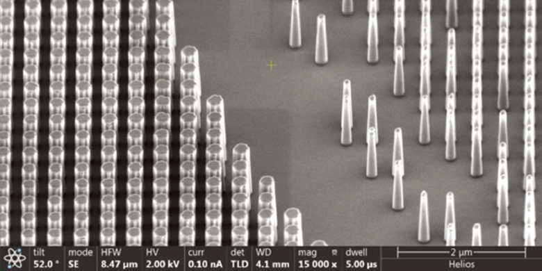
| ICP1 / ICP2 | High-Density Plasma | Compound semiconductors, high-aspect-ratio structures | Good sidewall control, tunable damage |
| IBE | Ion Beam Etching | Metals, alloys, inert materials | Pure physical bombardment, material-agnostic |
|
Deep Silicon Etcher |
Bosch Process | MEMS deep trenches, TSV through-holes | High aspect ratio, controllable scalloping |
|
Deep Dielectric Etcher |
Thick Film Dielectric Etching |
Thick oxide, glass vias | High selectivity, low mask loss |
|
Vapor Release Etcher |
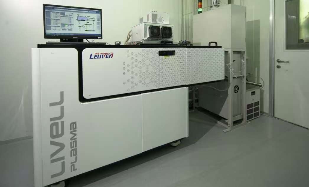
Vapor HF | Sacrificial layer release (MEMS structural release) | No liquid surface tension, anti-stiction |
8-inch and below wafers
Irregular samples and offcuts
Small batches, multiple varieties—the norm in R&D