Not with glue. Not with screws. Under specific conditions, they are brought together by van der Waals forces, molecular forces, or even atomic forces – a process called bonding.
Bonding is a critical step in MEMS manufacturing. It directly determines a device's mechanical stability, hermeticity, and overall functionality. The process requires atomically clean and flat wafer surfaces – and it is precisely this level of precision that enables high-performance microelectronic devices.
Plutosemi has mastered multiple bonding technologies, with process maturity sufficient to meet diverse customer requirements regarding substrate materials, thickness, temperature, and pressure. Whether you need standard bonding services or customized process development, we welcome the opportunity to collaborate.
Step 1: Surface Preparation
Try gluing two pieces of glass together when both are covered in dust and grease – it won't hold. Wafer bonding works on the same principle, only the requirements are thousands of times more demanding.
Through chemical cleaning and plasma activation, we thoroughly remove surface contaminants, achieving atomic-level cleanliness and flatness. Poor surface preparation renders all subsequent work futile.
Step 2: Alignment
The two wafers are precisely aligned under a microscope. For multi-layer devices, this step directly determines final performance – a miss by a micron is as good as a mile.
Alignment accuracy must reach the sub-micron level – a fundamental requirement of the bonding process.
Step 3: Bonding & Curing
Different material combinations and application scenarios call for completely different bonding processes. Some require high temperature, some require electric field assistance, and others need only gentle pressure.
The most appropriate bonding method is selected based on material characteristics and application requirements – the right choice makes all the difference.
Step 4: Inspection & Testing
Every batch undergoes rigorous inspection after bonding.
Using scanning acoustic microscopes and other equipment, we examine the bonding interface for voids or defects. These defects are invisible to the naked eye, but if present, they can cause complete device failure. Batch-by-batch inspection ensures every wafer meets quality standards.

Leveraging its mature MEMS process platform, Plutosemi offers the following seven bonding technologies.
Anodic Bonding – Bonding of silicon to glass using electric field assistance, requiring no intermediate layer, with excellent hermeticity. Typical applications include pressure sensors and inertial sensor packaging.
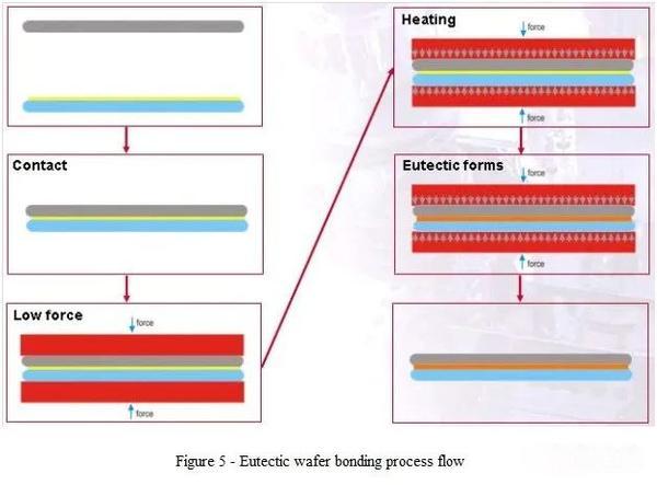
Eutectic Bonding – Forms a eutectic alloy layer (Au-Si, Au-Ge, Al-Ge, Au-Sn, Au-In, etc.), offering high bond strength and excellent hermeticity. Suitable for wafer-level hermetic packaging and RF devices.
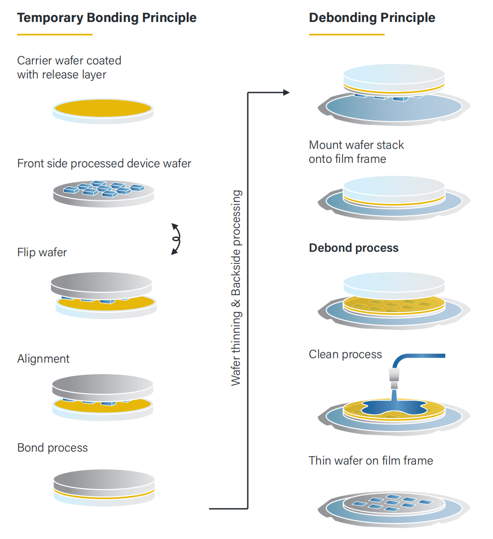
Adhesive Bonding – Uses specialized adhesives (AZ4620, SU8, etc.), with low process temperature, suitable for both temporary and permanent bonding. Ideal for temporary bonding and multi-layer structure integration.
Wire Bonding – Uses heat, pressure, and ultrasonic energy to interconnect metal wires with bond pads. Applied to electrical connections between chips and external circuits.
Silicon-Silicon Direct Bonding – Requires no intermediate layer, achieves direct bonding through high-temperature annealing, resulting in a pure interface and high mechanical strength. Typical applications include SOI substrate manufacturing and 3D integration.
Flip-Chip Bonding – The active side of the chip faces downward and interconnects with the substrate via solder bumps, offering short interconnection paths and low parasitic parameters. Suitable for high-density packaging and advanced packaging.
Multi-Layer Bonding – Stacking and bonding three or more wafers. Process control is more challenging, but the increase in integration density is significant. Suitable for complex MEMS structure stacking and 3D integration.