Thin Film Deposition Process Service: 8-inch Wafers · 70nm Lift-off Line Width
What is Thin Film Deposition?
Simply put, thin film deposition is the process of "coating" a nano-scale thin film layer onto a wafer.
It is a fundamental skill in micro-nano fabrication, yet it determines the upper limit of device performance. The film, ranging in thickness from a few nanometers to several micrometers, can serve as:
Insulating Layer: Keeping circuits isolated
Conductive Electrode: Providing electrical interconnection for the chip
Hard Mask: Aiding the etching process as a protective stencil
Optical Film: Enhancing transmission or reflection for optical devices
Thin Film Deposition Primarily Falls into Two Categories
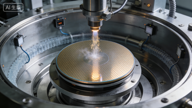
Chemical Vapor Deposition (CVD)
A film "grows" on the substrate surface through chemical reactions, suitable for dielectric materials such as silicon oxide and silicon nitride. This method is akin to applying a nourishing mask – slow and permeating.
Physical Vapor Deposition (PVD)
Materials are "sputtered" or "evaporated" onto the substrate using physical methods, including magnetron sputtering and electron beam evaporation. Suitable for metals and alloys such as gold, silver, and titanium – as clean and crisp as spray painting.
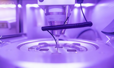
Our Process Capabilities
With years of experience in the thin film deposition field, we offer deposition processing services for various wafers and pieces up to 8 inches, with a comprehensive range of materials.
CVD Process Dielectric Thin Films
Silicon oxide, silicon nitride – available as needed.
PVD Process Metal Thin Films
Gold, silver, aluminum, titanium, nickel, chromium – metal oxide and alloy films can also be customized upon request.
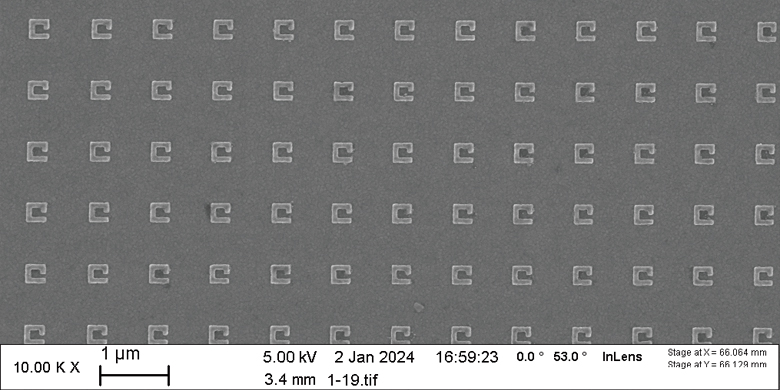
Process Highlight
Deposition-lift-off line width achievable down to 70nm – meeting high-precision patterning requirements and capturing the finest details.
Equipment Configuration
| Equipment |
Quantity |
| PECVD Deposition System |
2 units |
| Magnetron Sputtering System |
2 units |
| Electron Beam Evaporator |
1 unit |
| Optical Coating System |
1 unit |
| Rapid Thermal Annealing (RTA) Furnace |
1 unit |
| Tube Annealing Furnace |
1 unit |
| Semi-automatic Cleaner |
1 unit |
| Wafer Dryer |
1 unit |
Whether you are from a university research group or a corporate R&D center, feel free to reach out. We can help you avoid some detours along the way.
Contact
Lance Xie
Email: lance@plutosemi.com
PlutoSemi


