One Material, Infinite Patterns – PI Patterning Explained
Did you know there is a material that can withstand extreme cold of -269°C and short-term heat up to 400°C ?
It is PI (Polyimide), the "engineering material all-rounder" in the MEMS world. Aerospace, microelectronics, and laser applications cannot do without it. We are a team with more than 10 years of MEMS process experience, and today we are going to talk about the PI patterning process.
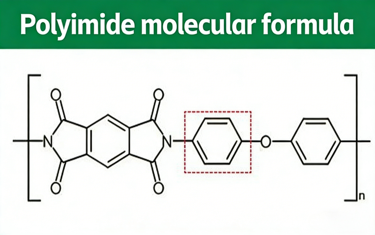
First, a quick introduction: What is PI?
Simply put, it is formed by the polycondensation of PMDA and DDE in a strong polar solvent, followed by imidization.
Its properties are outstanding:
Extreme cold resistance: stable at -269°C
High temperature resistance: long-term use at 280°C, short-term up to 400°C
Electrical insulation + dielectric resistance + strong adhesion + high mechanical strength + radiation resistance
That is why it appears in high-end fields such as aerospace, aviation, microelectronics, nanotechnology, liquid crystals, separation membranes, and lasers.
So, what exactly is the "PI patterning process"?
It means "engraving" precise patterns on thick PI films.
The typical process flow is as follows:
Coating / lamination – spin-coating non-photosensitive PI solution or laminating dry film
Exposure – UV light through a mask to define the pattern
Development – removing exposed or unexposed areas (depending on positive/negative resist)
Etching – controllable depth: up to 15μm for dry film, up to 21μm for non-photosensitive solution
Stripping / curing – removing residual photoresist and high-temperature imidization for final shaping
With thick-film patterning, we can create complex structures such as deep trenches, microchannels, 3D insulation layers,
and sensor supports. It is widely used in MEMS sensors, microfluidic chips, power devices, flexible electronics, and more.
What can our team do?
There are two mainstream PI processing methods in MEMS: dry film and adhesive type (non-photosensitive solution).
Process capability at a glance:
Dry film: thickness 20–200μm, etching depth up to 15μm
Non-photosensitive solution: etching depth 0–21μm (flexible control)
We are not just about process – we are your technology partner from design to mass production.
Interested? Please contact:
sales@plutosemi.com Lance