Silicon Lenses: The Unsung Heroes of IR & Laser Tech
Driven by IR imaging and LiDAR, Silicon Lenses are rapidly replacing expensive Germanium optics due to their high refractive index, low density, and cost-efficiency. However, achieving nanoscale surface accuracy on brittle silicon remains the ultimate manufacturing bottleneck.
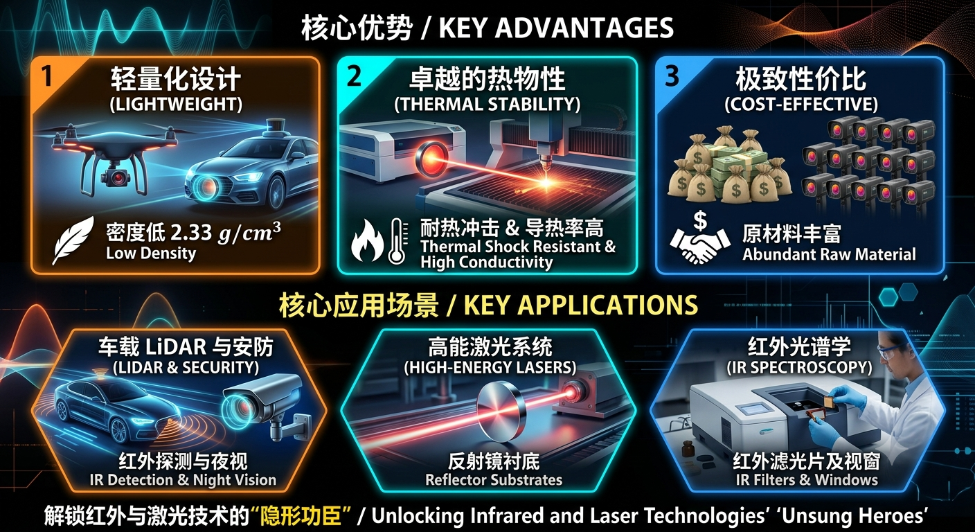
In infrared (IR) and high-energy laser applications, traditional glass optics fall short. Monocrystalline Silicon Lenses have become indispensable in the Mid-Wave Infrared (MWIR, 1.2 - 7μm) band due to their exceptional physical properties.
Key Advantages & Applications
Lightweight:Density is half that of Germanium, making it ideal for weight-sensitive autonomous driving and drone cameras.
Thermal Stability:High thermal conductivity prevents optical distortion in high-power carbon dioxide laser systems and harsh environments.
Cost-Effective:Abundant raw material reserves make it far more suitable for mass-producing consumer-grade thermal imagers than costly Germanium.
Manufacturing Bottlenecks
Lattice Distortion:As a brittle material, Silicon is prone to micro-cracks. Lattice distortion can spike laser absorption, causing catastrophic failure under high power.
Anti-Reflection coating:An uncoated Silicon surface suffers a ~30% reflection loss. Advanced BBAR or DLC coatings are mandatory to push transmission past 90%.
Looking Ahead
As autonomous driving and industrial IR sensors proliferate, the demand for precision aspheric Silicon lenses is hitting an inflection point. Moving forward, breakthroughs in molded Silicon technology will be key to unlocking its full commercial potential.