3D NAND Process Overview: From Raw Silicon to Advanced Package
If logic chips build a flat "transportation network" on silicon, 3D NAND erects multi-hundred-story "skyscrapers" at the nanoscale. Its process flow pushes front-end deposition, ultra-high aspect ratio etching, and back-end advanced packaging to their absolute limits:
FEOL: Substrate & CMOS Foundation
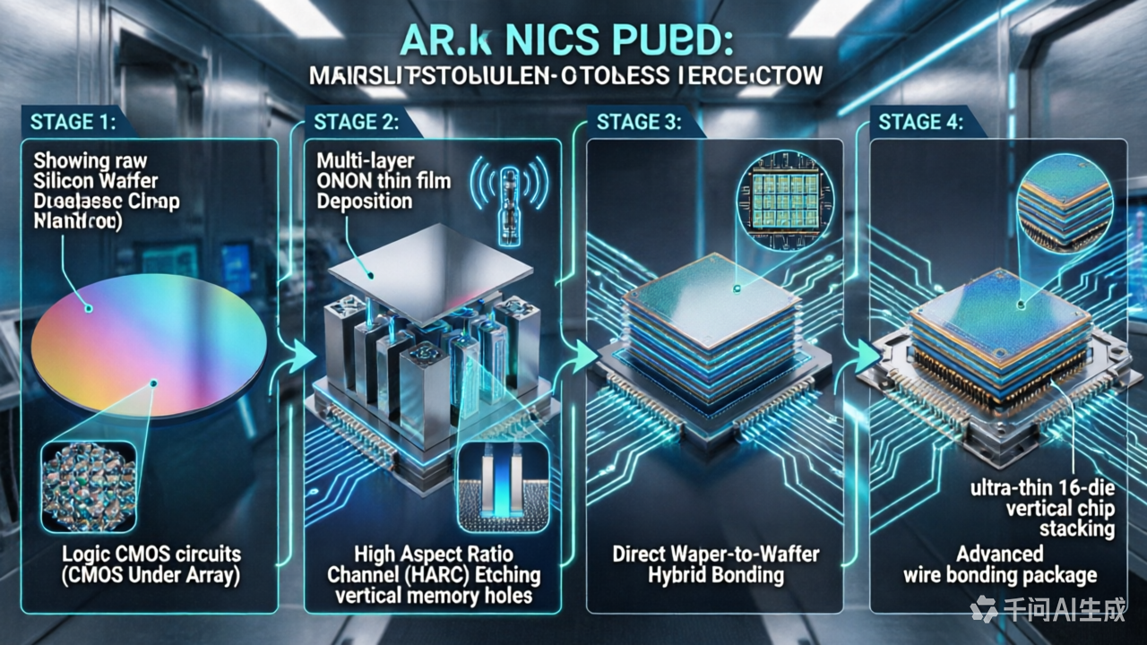
Wafer Prep & Circuitry:After polishing the raw wafer, the peripheral control circuits are built first (CMOS Under Array, or CuA architecture) to save die area by placing logic directly beneath the memory array.
MEOL: 3D Memory Array Fabrication
Alternating Layer Deposition:Alternating CVD/ALD deposits hundreds of alternating oxide and nitride (ONON) film layers.
HARC Etching:HARC Etching: Pushing physical limits! Dry plasma etching punches through hundreds of layers to create channel holes with aspect ratios exceeding 70:1.
Gate-Replacement & Metallization:Sacrificial nitride layers are etched away and replaced with tungsten (W) or molybdenum (Mo) metal to form Word Lines.
Wafer-Level Integration
Direct Wafer-to-Wafer Bonding:Wafer-to-Wafer Hybrid Bonding: In architectures like Xtacking®, the memory array wafer and logic wafer are aligned and fused at room temperature via nano-scale Cu-Cu hybrid bonding.
BEOL: Thinning, Dicing & Packaging
Wafer Thinning & Dicing:Wafers are thinned down to tens of micrometers (thinner than a human hair) and diced into individual 3D NAND dies.
Die Stacking & Interconnect:8- or 16-die stacks are vertically assembled, connected via wire bonding or TSVs, and encapsulated in protective resin.
Conclusion
From a basic silicon substrate to a high-density wafer hosting billions of vertical memory cells, and finally to an ultra-thin multi-die package—3D NAND process evolution epitomizes the ultimate synergy of materials science, plasma physics, and micro-engineering.