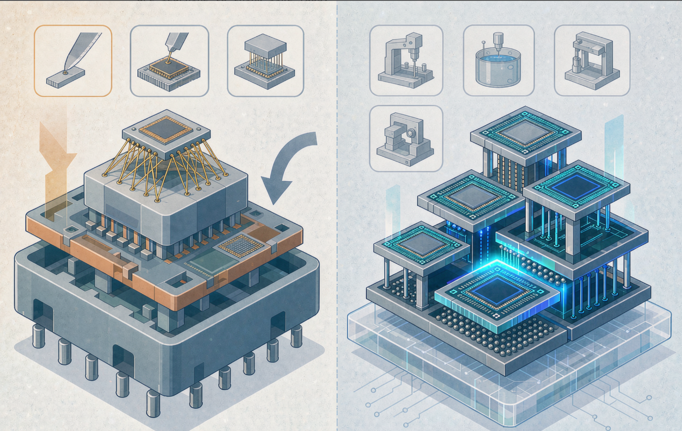
1 、Say packaging and most people still think back-end: dicing, die attach, bonding, molding. Yet todays advanced packaging lines run lithography, PVD, plating and CMP — and their engineers watch SPC trends and process windows.Packaging is starting to look a lot less like packaging.Lets discuss: will advanced packaging swallow traditional OSATs, or can they genuinely evolve into mini-fabs?
2 、Just look at the process list. RDL runs lithography, development, PVD, seed layer, plating, etching, resist stripping and cleaning. TSV runs deep-via etch, insulation, barrier, seed, plating fill and CMP. Fan-Out needs temporary bonding, reconstituted wafers, multi-layer routing and warpage control. 2.5D/3D needs microbumps, hybrid bonding and high-precision alignment. Glass substrates and TGV add laser drilling, via metallization and reliability verification.Traditional packaging competed on assembly capability. Advanced packaging competes on micron — even sub-micron — process control.
3 、As RDL line width and spacing shrink, litho alignment, copper plating thickness, line-edge profile, resist residue, particles and film adhesion all bear directly on reliability. TSV fill is even less forgiving — poor wetting, a discontinuous seed layer or an imbalanced plating bath produces voids, seams and abnormal stress. Hybrid bonding is the most sensitive of all: a single particle can cause local bonding failure.This is no longer a question of did it sit straight or did it solder well. Engineers have to think like fab engineers: SPC trends, defect distribution, film-thickness uniformity, particle sources, process windows, equipment state, and the coupling between upstream and downstream steps. Cleanliness control, DOE, metrology feedback, yield analysis, closed-loop excursions, change management — you need all of it.
4 、Final Thoughts
When packaging starts thinking like a fab, the industry map gets redrawn. The next decades competitiveness wont be about whose line is bigger — itll be about who can hold a narrower process window and still stay stable.