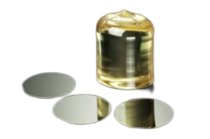
| Parameter | Specification |
| Material | LiTaO3 wafers(White or Black &Fe doped) |
| Diameter | 3inch/4inch/6inch |
| Diameter Tolerance | ±0.03mm |
| Curie Temp | 603±2℃ |
| Cutting Angle | X/Y/Z/X112Y/Y36/Y42/Y48/etc |
| Tol(±) | <0.20 mm |
| Thickness | 0.18 ~ 0.5mm or more |
| Primary Flat | 22mm /32mm /42.5mm /57.5mm |
| LTV (5mmx5mm) | <1µm |
| TTV | <3µm |
| BOW | -30 |
| WARP | <40µm |
| PLTV(<0.5um) | ≥95%(5mm*5mm) |
| Orientation Flat | All available |
| Surface Type | Single Side Polished(SSP) /Double Sides Polished(DSP) |
| Polished side Ra | <0.5nm |
| Back Side Criteria | General is 0.2-0.5µm or as customized |
| Edge Criteria | R=0.2mm or Bullnose |
| Fe doped | Fe doped for saw grade LN< wafers |
| Wafer Surface Criteria | |
| Contamination None | |
| Particles @>0.3 µm ≤30 | |
| Scratch , Chipping None | |
| Defect No edge cracks, scratches, saw marks, stains | |
| Packing | 25pcs per box |
Optical Grade Lithium Tantalate Wafers
| Parameter | Specification |
| Material | LiTaO3 wafers(White or Black) |
| Diameter | 2inch/3inch/4inch |
| Diameter Tolerance | ±0.03mm |
| Curie Temp | 603±2℃ |
| Cutting Angle | X/Y/Z etc. |
| Tol(±) | <0.20 mm |
| Thickness | 0.18 ~ 0.5mm or more |
| Primary Flat | 16mm/22mm /32mm |
| TTV | <3µm |
| BOW | -30 |
| WARP | <40µm |
| Surface Type | Single Side Polished(SSP) /Double Sides Polished(DSP) |
| Polished side Ra | <0.5nm |
| Back Side Criteria | General is 0.2-0.5µm or as customized |
| Edge Criteria | R=0.2mm or Bullnose |
| Optical doped | Zn/MgO etc. |
| Wafer Surface Criteria | |
| Particles @>0.3 µm ≤30 | |
| Scratch , Chipping None | |
| Defect No edge cracks, scratches, saw marks, stains | |
| Packing | 25pcs per box |
SAW Grade Lithium Tantalate Wafers
| Parameter | Specification |
| Material | LiTaO3 wafers |
| Diameter | 3inch/4inch/6inch |
| Diameter Tolerance | ±0.03mm |
| Curie Temp | 603±2℃ |
| Cutting Angle | X/Y/Z/X112Y/Y36/Y42/Y48/etc. |
| Tol(±) | <0.20 mm |
| Thickness | 0.18 ~ 0.5mm or more |
| Primary Flat | 22mm /32mm /42.5mm /57.5mm |
| LTV (5mmx5mm) | <1µm |
| TTV | <3µm |
| BOW | -30 |
| WARP | <40µm |
| PLTV(<0.5um) | ≥95%(5mm*5mm) |
| Orientation Flat | All available |
| Surface Type | Single Side Polished(SSP) /Double Sides Polished(DSP) |
| Polished side Ra | <0.5nm |
| Back Side Criteria | General is 0.2-0.5µm or as customized |
| Edge Criteria | R=0.2mm or Bullnose |
| Wafer Surface Criteria | |
| Contamination None | |
| Particles @>0.3 µm ≤30 | |
| Scratch , Chipping None | |
| Defect No edge cracks, scratches, saw marks, stains | |
| Packing | 25pcs per box |
