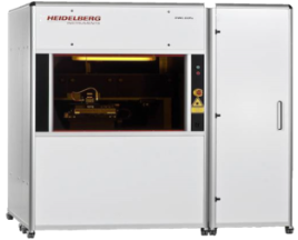
Laser Direct Writing System | Heidelberg Instruments DWL66+
Capabilities:
Advanced laser lithography system enabling high-precision micro/nano structure patterning with 300 nm minimum feature size. Ideal for prototyping and small-batch production of photonic devices, MEMS, and specialized semiconductor structures.
Technical Specifications:
Minimum feature size: 300 nm
Writing grid: 7 nm
Line edge roughness: 50 nm
Linewidth uniformity: 60 nm
Overlay accuracy: ≤100 nm
Writing speed: 3 mm²/min
Process Advantages:
High-resolution patterning without mask requirements
Excellent linewidth control and edge definition
Flexible direct-write capability for rapid prototyping
Superior overlay accuracy for multi-layer structures
Primary Applications:
Photonic device fabrication
MEMS and sensor prototyping
Specialized semiconductor structures
Research and development lithography
Why Choose Our Service?
We provide high-precision direct-write lithography with 300 nm resolution and ≤100 nm overlay accuracy. Our maskless process enables rapid prototyping and flexible patterning for your photonic, MEMS, and specialized semiconductor applications. Partner with us to accelerate your device development with reliable, high-quality lithography solutions.