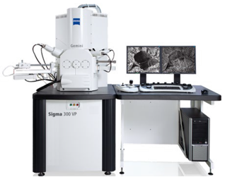
30kV Electron Beam Lithography System | ZEISS Sigma 300
Capabilities:
Advanced electron beam lithography system delivering ultra-high resolution patterning down to 50 nm minimum feature size. With 30 kV acceleration voltage and precise field stitching capability, this system enables nanoscale lithography for research and development of cutting-edge semiconductor devices, photonic components, and nano-electromechanical systems.
Technical Specifications:
Wafer compatibility: up to 4-inch
Acceleration voltage: 30 kV
Maximum write field: 2 × 2 mm²
Minimum linewidth: ≤50 nm
Overlay accuracy: ≤50 nm
Field stitching accuracy: ≤100 nm
Process Advantages:
Ultra-high resolution patterning without mask requirements
High acceleration voltage enables precise pattern definition
Excellent field stitching accuracy for large-area patterning
Superior overlay accuracy for multi-layer device fabrication
Primary Applications:
Research and development of advanced semiconductor devices
Photonic and plasmonic device fabrication
Nano-electromechanical systems (NEMS)
Quantum device patterning
Why Choose Our Service?
We provide nanoscale patterning with 50 nm resolution and 50 nm overlay accuracy using high-voltage electron beam technology. Our system's precise field stitching and maskless capability enable rapid prototyping of your most advanced device concepts. Partner with us to push the boundaries of nanofabrication and accelerate your cutting-edge research and development projects.