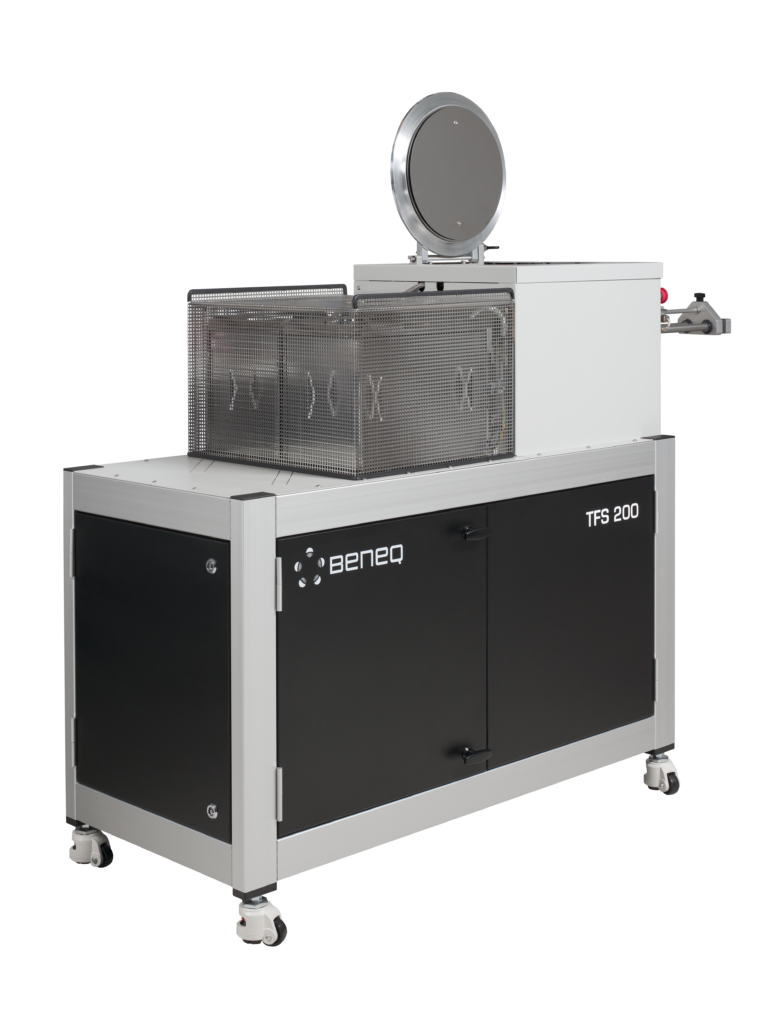
Atomic Layer Deposition (ALD) System | Beneq TFS 200
Capabilities:
Advanced ALD system enabling precise deposition of high-quality thin films including Al₂O₃, HfO₂, TiO₂, SiO₂, AlN, and SiNₓ. Combining RF and thermal reaction technologies for superior film conformity and step coverage, ideal for semiconductor devices, MEMS, and advanced packaging applications.
Technical Specifications:
Integrated ozone generator
Automated loadlock chamber
Dual reaction modes: RF + thermal
Maximum sample size: 8 inches
Substrate temperature control accuracy: ±1°C
Maximum substrate temperature: 500°C
Maximum precursor temperature: 300°C
Process Advantages:
Exceptional film uniformity and conformity through self-limiting surface reactions
Precise thickness control at atomic level with ±1°C temperature stability
Wide material selection enabled by dual reaction mechanisms
High-quality dense films achieved through 500°C substrate heating capability
Primary Applications:
High-k gate dielectrics in semiconductor devices
Surface passivation layers for MEMS and sensors
Protective and functional coatings for optical components
Diffusion barriers in advanced interconnect structures
Why Choose Our Service?
We deliver atomically precise thin films with superior conformity and thickness control using advanced ALD technology. Our system's dual reaction capability and 500°C processing temperature ensure high-quality dielectric and nitride films for your most demanding semiconductor and MEMS applications. Partner with us to achieve reliable, uniform coatings that enhance device performance and reliability.