
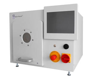
A high-performance microwave plasma system engineered for precise, residue-free dry photoresist stripping and effective surface activation of diverse materials. Ideal for semiconductor fabrication, MEMS processing, and advanced material research.
Dry Photoresist Stripping: Complete removal of various photoresist types without wet chemicals.
Surface Activation & Cleaning: Enhances surface energy for improved adhesion in bonding and coating processes.
Plasma Treatment: Utilizes O₂, Ar, and CF₄ gases for versatile surface modification.
Maximum Wafer Size: 8 inches
Ultimate Vacuum: <20 mTorr
Process Gases: O₂, Ar, CF₄
Temperature-Controlled Stage: 60-200°C (adjustable)
Microwave Power Frequency: 2.45 GHz
Microwave Power Range: 0–600 W (continuously adjustable)
Gentle yet Thorough Stripping: Low-temperature, isotropic plasma process protects delicate structures and substrates.
Exceptional Uniformity: Controlled microwave plasma and heated stage ensure consistent results across the entire wafer.
Eco-Friendly Operation: Dry process eliminates the need for hazardous wet chemicals, reducing waste and cost.
High Versatility: Easily configurable for both stripping and activation applications with flexible gas and power settings.
Semiconductor device manufacturing
MEMS and sensor fabrication
Advanced packaging and 3D integration
R&D laboratories for new materials and process development
Surface preparation for thin-film deposition and bonding
Why Choose Our Service?
We deliver precise dry photoresist stripping and surface activation using advanced microwave plasma technology. Our system ensures residue-free cleaning and uniform treatment for wafers up to 8 inches, with flexible gas options (O₂, Ar, CF₄) and tunable power (0–600 W). Through eco-friendly, low-temperature processes, we protect sensitive structures while enabling rapid development cycles for semiconductor, MEMS, and advanced packaging applications. Partner with us to achieve reliable, high-quality surface preparation and accelerate your R&D and pilot production.

