
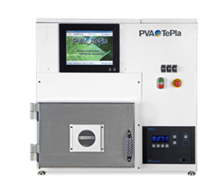
The PVA TePla IoN 40 is a robust RF plasma system engineered for high-efficiency photoresist stripping, residue removal, and surface preparation. It delivers exceptional cleaning and activation performance for semiconductor manufacturing, advanced packaging, and R&D applications.
Photoresist & Residue Stripping: Thoroughly removes photoresist and post-etch residues without damaging delicate wafer structures.
Surface Activation: Prepares surfaces for superior adhesion in bonding and packaging processes.
Surface Decontamination: Effectively cleans organic contaminants from various substrates.
Maximum Wafer Size: 8 inches
Ultimate Vacuum: 5.0 mTorr
Process Gases: O₂, Ar
Electrode System: 5-layer removable aluminum trays
RF Power Frequency: 13.56 MHz
RF Power Output: 0–600 W (continuously adjustable)
High Throughput Design: The 5-layer tray configuration enables batch processing, significantly boosting productivity.
Precision & Control: Industry-standard 13.56 MHz RF power with continuous adjustment allows for gentle yet complete cleaning.
Process Versatility: Supports both oxidative (O₂) and inert (Ar) plasma chemistries for a wide range of applications.
Reliable Performance: Engineered for consistent, repeatable results in demanding production environments.
Semiconductor device fabrication
Advanced packaging and 3D integration
MEMS and sensor manufacturing
Surface cleaning and activation for bonding
R&D and pilot production lines
We deliver high-efficiency plasma stripping and surface treatment using advanced RF plasma technology. Our batch processing system with 5-layer tray configuration ensures high throughput and uniform results for 8-inch wafers. With precise 13.56 MHz RF power control and dual-gas capability, we provide gentle yet complete photoresist removal and surface activation. Trust our expertise to accelerate your semiconductor, advanced packaging, and MEMS production with reliable, reproducible plasma processing solutions.

