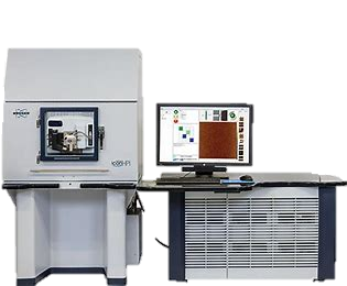
Atomic Force Microscope | Bruker Dimension Icon System
Capabilities:
The Bruker Dimension Icon atomic force microscope (AFM) obtains sample surface topography by detecting atomic-scale interactions between the probe and sample. Designed for high-resolution nanoscale imaging and characterization across multiple operational modes.
Technical Specifications:
Operational Modes: Multiple working modes
Key Function: Intelligent automatic probe approach
Noise Performance (closed-loop): Z-axis ≤ 0.035 nm (RMS), XY-axis ≤ 0.15 nm (RMS)
Thermal Drift Rate: < 0.2 nm/min
Vibration Isolation: Integrated anti-vibration and acoustic isolation system
Process Advantages:
High-resolution surface topography imaging at atomic scale
Multiple operational modes for versatile measurement requirements
Intelligent automatic probe approach enhances operational efficiency
Low-noise closed-loop control ensures measurement stability
Integrated vibration isolation maintains accuracy in varied environments
Primary Applications:
Surface topography imaging and nanoscale characterization through detection of atomic-scale interactions between probe and sample.
Why Choose Our Service?
Our expertise in atomic force microscopy delivers nanoscale surface characterization essential for your advanced material research and quality control. Using the Bruker Dimension Icon system, we provide high-resolution topography data and precise nanoscale measurements—supporting your surface analysis, material characterization, and process development with reliable AFM solutions tailored to your specific research and inspection requirements.