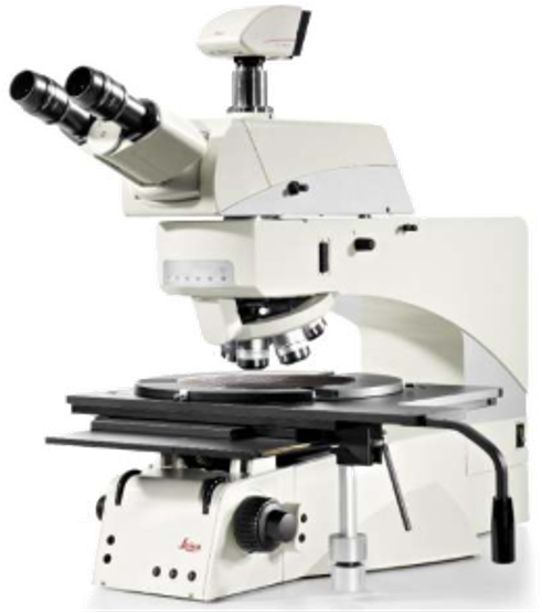
Metallurgical Microscope | Leica DM8000M System
Capabilities:
Our advanced metallurgical microscope enables semiconductor device feature dimension measurement, particle observation, and detection of misalignment and surface defects. Designed for high-precision imaging and inspection in semiconductor manufacturing and quality control applications.
Technical Specifications:
Imaging System: OEM color camera
Objective Nose piece: Motorized revolving nosepiece
Objective Lenses: 5 objectives (5× – 100× magnification)
Observation Modes: Brightfield, darkfield, differential interference contrast (DIC), polarized light, and transmitted light
Stage Travel Range: 200 mm (X direction), 200 mm (Y direction)
Software Functions: Image acquisition, manual measurement, annotation, and depth-of-field stacking
Process Advantages:
Multiple observation modes enable comprehensive defect detection
Motorized nosepiece allows fast, reproducible objective switching
Large stage travel range accommodates full wafer inspection
High-resolution color imaging captures fine feature details
Advanced software functions support precise dimensional analysis
Depth-of-field stacking extends focus range for topographic samples
Primary Applications:
Semiconductor device feature dimension measurement, particle observation, misalignment detection, and surface defect inspection in semiconductor manufacturing, packaging, and quality control.
Why Choose Our Service?
Partner with us for high-precision optical microscopy solutions that deliver the imaging clarity, measurement accuracy, and inspection capability your semiconductor processes demand. Using the Leica DM8000M system, we provide comprehensive defect detection, precise dimensional measurement, and expert technical support—helping you maintain process control, verify device features, and ensure product quality with inspection solutions tailored to your specific semiconductor device requirements.