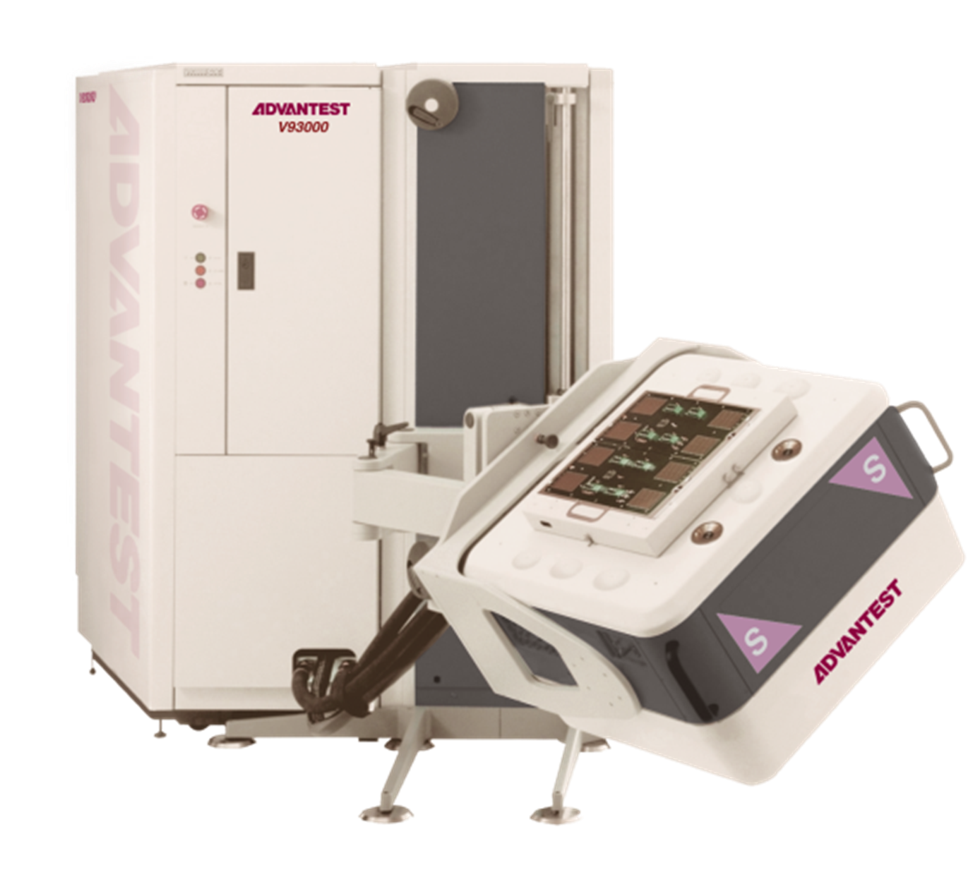
Semiconductor Test System | Advantest V9300 System
Capabilities:
Our advanced semiconductor test system integrates with automatic probers to perform functional and electrical parameter testing on bare dies during wafer-level inspection. Designed for high-throughput, precision characterization of semiconductor devices.
Technical Specifications:
Continuous Current Capability: 80 channels
High-Precision Voltage Measurement Units: 8 units
Waveform Generation: 8 channels AWG (Arbitrary Waveform Generator) and 8 channels DGT (Digital Generator)
Digital Signal Rate: 2.2 Gbps
Test Vector Depth: 1024 M
Force Voltage Accuracy: 1.5 mV
Channel-to-Channel Skew: < 56 ps
Process Advantages:
High channel count enables parallel testing for increased throughput
Dedicated high-precision voltage measurement units ensure accurate parametric testing
Integrated AWG and DGT support complex waveform generation requirements
High-speed digital interface accommodates advanced device protocols
Deep test vector memory supports comprehensive test program execution
Exceptional voltage accuracy delivers reliable, repeatable measurements
Ultra-low channel skew ensures precise timing-critical test execution
Primary Applications:
Functional and electrical parameter testing of bare dies during wafer-level inspection, in conjunction with automatic prober systems, for semiconductor device characterization and production test.
Why Choose Our Service?
Partner with us for advanced semiconductor test solutions that deliver the speed, accuracy, and channel density your wafer-level testing demands. Using the Advantest V9300 system, we provide comprehensive functional and parametric test capabilities, high-throughput parallel testing, and expert technical support—helping you accelerate time-to-market, reduce test cost, and ensure device quality with test solutions tailored to your specific semiconductor device requirements.