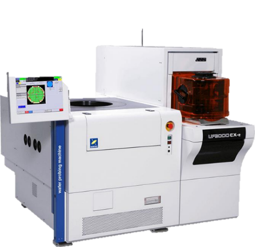
Automatic Probe System | Accretech AP3000e System
Capabilities:
Our advanced automatic probe system integrates with semiconductor testers to enable wafer-level inspection, device characterization, and failure analysis applications throughout wafer manufacturing and chip development.
Technical Specifications:
Probe Card Management: Automatic probe card exchange function
Data Output: Wafer map generation capability
Wafer Size Compatibility: 8-inch wafers
XY-Axis Resolution: 0.5 nm
Z-Axis Resolution: 0.167 μm
θ-Axis Resolution: 0.0000276°
Process Advantages:
Automatic probe card exchange reduces setup time and operator intervention
Wafer map output enables seamless data integration with test systems
Sub-nanometer XY positioning ensures precise alignment accuracy
High-resolution Z-axis control optimizes probe contact consistency
Ultra-fine θ-axis resolution delivers precise angular positioning
Dedicated 8-inch wafer compatibility supports mainstream production requirements
Primary Applications:
Wafer-level inspection, device characterization, and failure analysis in semiconductor manufacturing and chip development, operating in conjunction with test systems.
Why Choose Our Service?
Partner with us for high-precision automatic probing solutions that deliver the positioning accuracy, automation efficiency, and data integration your wafer testing demands. Using the Accretech AP3000e system, we provide exceptional alignment precision, automated probe card handling, comprehensive wafer mapping, and expert technical support—helping you maximize tester utilization, reduce manual intervention, and accelerate device characterization with probing solutions tailored to your specific wafer-level test requirements.