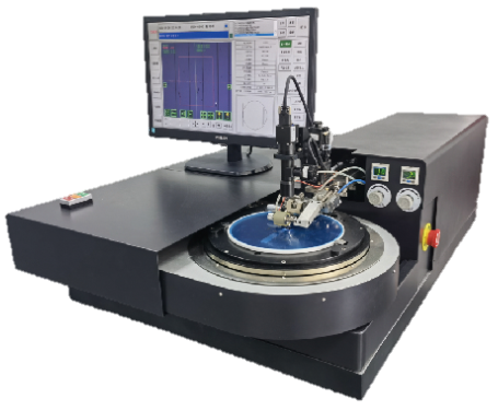
Cleaving System | Seiryo Electronics ESD-6306 System
Capabilities:
Our advanced cleaving system first creates a scribe mark at the wafer edge using a diamond blade, then applies roller pressure along the scribe line to fracture the wafer, separating it into individual bars along cleaving planes. Designed for precision compound semiconductor and MEMS device singulation.
Technical Specifications:
Process Integration: Integrated scribing and breaking in one system
Operation Mode: Automatic alignment and automatic cleaving
Wafer Size Compatibility: 6 inches and below
Scribe Blade Positioning Accuracy: ≤ 5 μm
Sample Rotation: 0–360°
Minimum Cleave Length: ≤ 250 μm
Process Advantages:
Integrated scribe-and-break design eliminates process transfer
Fully automatic operation ensures consistency and repeatability
High positioning accuracy delivers precise scribe placement
Full 360° rotation accommodates various crystal orientations
Ultra-small cleave length supports miniature device singulation
Dedicated small wafer format compatibility addresses compound semiconductor and R&D needs
Primary Applications:
Wafer cleaving along crystallographic planes to produce individual bars for compound semiconductor laser diodes, LEDs, MEMS, and other miniaturized devices.
Why Choose Our Service?
Partner with us for precision cleaving solutions that deliver accurate scribe placement, clean fracture surfaces, and automated operation. Using the Seiryo Electronics ESD-6306 system, we provide integrated scribe-and-break capability, sub-5 μm positioning, and expert support—helping you achieve consistent bar separation and improve yield with cleaving solutions tailored to your compound semiconductor and MEMS device singulation requirements.