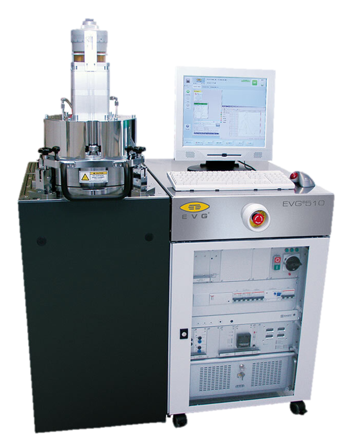
Wafer Bonder | EVG 510
Capabilities:
Our advanced wafer bonding system enables wafer-to-wafer (W2W) bonding processes including anodic bonding, silicon direct bonding, metal thermocompression bonding, and eutectic bonding. Designed for MEMS, compound semiconductor, and advanced packaging applications.
Technical Specifications:
Bonding Chamber: High vacuum bonding chamber
Thermal Module: Rapid heating module
Wafer Size Compatibility: 2, 4, 6-inch wafers
Maximum Bonding Force: 60 kN
Heating Temperature Range: Room temperature – 500°C (top and bottom substrates)
Bonding Processes: Anodic, eutectic, thermocompression, silicon direct bonding, and more
Process Advantages:
High vacuum chamber ensures contamination-free bonding interfaces
Rapid heating module reduces thermal budget and cycle time
High bonding force accommodates diverse process requirements
Broad temperature range supports multiple bonding techniques
Multi-size wafer compatibility enables flexible production
Primary Applications:
Wafer-to-wafer anodic bonding, silicon direct bonding, metal thermocompression bonding, and eutectic bonding for MEMS fabrication, compound semiconductor processing, and advanced packaging.
Why Choose Our Service?
Partner with us for wafer bonding solutions that deliver process versatility, high vacuum integrity, and precise thermal control. Using the EVG510 system, we provide reliable anodic, direct, thermocompression, and eutectic bonding capabilities—helping you achieve strong, void-free wafer interfaces with bonding solutions tailored to your specific device layer transfer and 3D integration requirements.