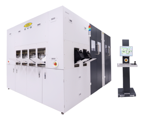
Wafer Hybrid Bonding System | EVG Gemini FB
Capabilities:
Our advanced wafer hybrid bonding system enables wafer-to-wafer (W2W) anodic bonding, silicon direct bonding, metal thermocompression bonding, and eutectic bonding processes. Fully automated wafer cleaning, activation, alignment, bonding, and inspection are integrated within a single platform.
Technical Specifications:
Wafer Size Compatibility: 6, 8-inch wafers
Alignment Accuracy: ≤ 100 nm
Post-Bonding Accuracy: ≤ 200 nm
Process Integration: Fully automated wafer cleaning, activation, alignment, bonding, and inspection
Process Advantages:
Sub-100 nm alignment accuracy enables advanced node device integration
Tight post-bonding overlay precision ensures high-yield hybrid bonding
Fully automated process flow minimizes handling and contamination
All-in-one platform eliminates process interruptions and transfer delays
6 and 8-inch wafer compatibility supports production flexibility
Primary Applications:
Wafer-to-wafer anodic bonding, silicon direct bonding, metal thermocompression bonding, and eutectic bonding for advanced packaging, 3D integration, CMOS image sensors, and memory stacking applications
Why Choose Our Service?
Partner with us for hybrid wafer bonding solutions that deliver nanometer-scale alignment, fully automated process integration, and exceptional post-bonding accuracy. Using the EVG Gemini FB system, we provide reliable anodic, direct, thermocompression, and eutectic bonding capabilities—helping you achieve high-yield, high-throughput wafer stacking with bonding solutions tailored to your most demanding 3D integration and advanced packaging requirements.