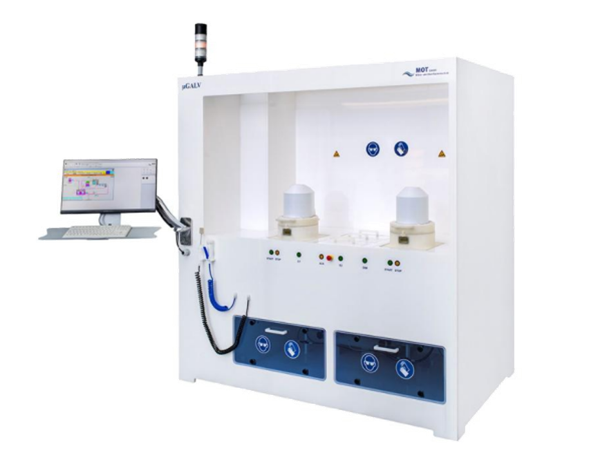
Wafer Plating System | MOT pGALV-R&D+
Capabilities:
Our advanced wafer plating system utilizes electroplating processes to form Pillar, RDL, TSV and other structures on wafer surfaces or within deep vias. Designed for advanced packaging, 3D integration, and MEMS applications.
Technical Specifications:
Power Supply: Pulsed DC power supply
Process Capability: TSV copper plating process solution
Wafer Size Compatibility: 4, 6, 8-inch wafers
Process Control: Plating solution flow rate control
Plating Uniformity: ≤ 5%
Platable Metals: TSV (Cu), Cu, Au, Ni, SnAg
Process Advantages:
Pulsed DC power supply enables precise deposition control
Dedicated TSV copper plating solution supports high aspect ratio via filling
Multiple wafer size compatibility provides production flexibility
Flow rate control ensures uniform mass transfer across wafer surface
≤5% uniformity delivers consistent film thickness distribution
Broad metal selection accommodates diverse application requirements
Primary Applications:
Electroplating of Pillar, RDL, TSV and other structures on wafer surfaces or within deep vias for advanced packaging, 3D IC integration, MEMS, and compound semiconductor device fabrication.
Why Choose Our Service?
Partner with us for wafer plating solutions that deliver exceptional uniformity, versatile metal capability, and dedicated TSV process support. Using the MOT pGALV-R&D+ system, we provide precise pulsed DC deposition, uniform film distribution, and expert technical support—helping you achieve void-free via filling and reliable interconnect formation with plating solutions tailored to your specific advanced packaging and 3D integration requirements.