
Our advanced photoluminescence scanning system analyzes epitaxial layer properties including luminescence uniformity, film thickness uniformity, and reflectance. Designed for compound semiconductor epitaxy characterization and quality control applications.
Minimum Resolution: 0.1 nm
Scan Spatial Resolution: 100 μm
Wavelength Range: 400 – 2040 nm
Sample Compatibility: 2-inch to 6-inch wafers and irregular fragments
Measurement Functions: Peak wavelength, integrated intensity, peak intensity, full width at half maximum (FWHM), and more.
High spectral resolution enables precise peak identification
100 μm spatial resolution captures detailed uniformity mapping
Broad wavelength range covers UV to NIR for multiple material systems
Flexible sample support accommodates full wafers and fragments
Comprehensive PL parameters provide complete epitaxial quality assessment
Analysis of epitaxial layer luminescence uniformity, film thickness uniformity, and reflectance for compound semiconductor materials in R&D and production environments.
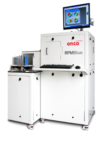
Partner with us for photoluminescence scanning solutions that deliver high-resolution spectral data, detailed uniformity mapping, and flexible wafer compatibility. Using the ONTO RPMblue system, we provide accurate peak wavelength, intensity, and FWHM measurements—helping you monitor epitaxial quality, optimize growth processes, and ensure material performance with characterization solutions tailored to your specific compound semiconductor requirements.

