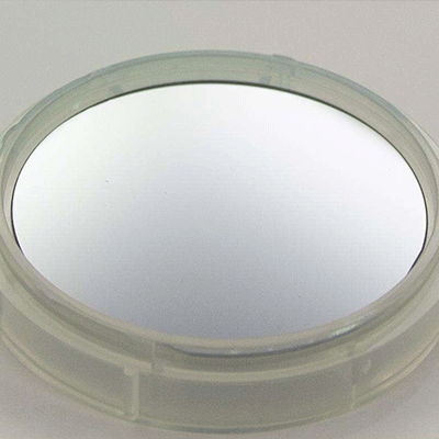
GaAs Substrate Wafers Gallium Arsenide(GaAs) is a semiconductor material with various exceptional properties such as direct band gap, high electron mobility, high frequency with less noise, and high conversion efficiency.As a result.the compound is an important fundamental material in the optoelectronic and microelectronic industries.In the optoelectronics field,GaAs is used in the manufacturing of LED(Light Emitting Diode),LD(Laser Diode).photovoltaic devices, etc, In the microelectronics fieid, GaAs is used in manufacturing of MESFET(metal semiconductor field-effect transistor),HEMT(High Electron Mobility Transistor),HBT(Hetero junction Bipolar Transistor). IC, Hall element, etc.
Gallium arsenide (GaAs) is the most important and most widely used semiconductor material in compound semiconductors, and also the most mature and most widely produced compound semiconductor material.
Advantages:
Gallium arsenide has high electron mobility (5-6 times that of silicon),
The band gap width is large (it is 1.43eV, silicon is 1.1eV), and the operating temperature can be higher than silicon
For direct band gap, good photoelectric characteristics, can be used as light and laser devices
Easily made half of insulating material (resistivity Ω 107-109 cm),
Low intrinsic carrier concentration
Good heat and radiation resistance
Sensitivity to magnetic field
It is easy to pull out single crystal
Gallium arsenide is a compound formed by combining gallium metal with semi-metallic arsenic in atomic ratio of 1:1. It has a gray metallic luster and its crystal structure is sphalerite type. Gallium arsenide was synthesized as early as 1926. By 1952 its semiconducting properties had been confirmed.
The device made of gallium arsenide material has good frequency response, high speed and high operating temperature, which can meet the needs of integrated optoelectronics. It is the most important optoelectronic material and the most important microelectronic material after silicon. It is suitable for making high frequency and high speed devices and circuits.
Gallium arsenide in our daily life in some applications: we now watch TV, listen to audio, air conditioning are all using remote control. These remote controls transmit instructions to the host via infrared light emitted by gallium arsenide. On many home appliances there are small red, green indicators, they are made of gallium arsenide and other materials as the substrate of light-emitting diodes. CDS and VCDS and DVDS are read out by laser diodes made of gallium arsenide as a substrate.
In recognition of its excellent performance and strategic significance, gallium arsenide (gaas) material devices and applications have been studied and developed continuously, which has laid a foundation for today's great development. Gallium arsenide devices have discrete devices and integrated circuits. Now integrated circuit is not the unified world of silicon, gallium arsenide integrated circuit has an important share of the IC market.
Gallium arsenide devices in use include:
Microwave diode, gunn diode, varsity diode, etc.
Microwave transistor: field effect transistor (FET), high electron mobility transistor (HEMT), heterojunction bipolar transistor (HBT), etc.
Integrated circuits: microwave monolithic integrated circuit (MMIC), ultra-high speed integrated circuit (VHSIC), etc.
Hall element
Infrared light-emitting diode (IR LED); Visible light emitting diode (LED);
Laser diode (LD);
Light detector;
Efficient solar cells;

