In today’s era of rapid smart technology and IoT (Internet of Things) advancement, non-contact temperature measurement has become essential across diverse fields like medical, industrial, consumer electronics, and security.
Thermopile MEMS sensors, with their unique advantages, are emerging as a leading technology in this market, powered by sophisticated semiconductor MEMS fabrication processes.
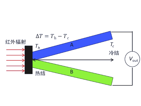
Core Principle: Based on the Seebeck effect. When a temperature difference exists between the two junctions (hot junction and cold junction) of two dissimilar conductors or semiconductors(forming a thermocouple), a thermoelectric voltage (emf) is generated. A thermopile is a structure where multiple thermocouples are connected in series to amplify the output voltage signal.
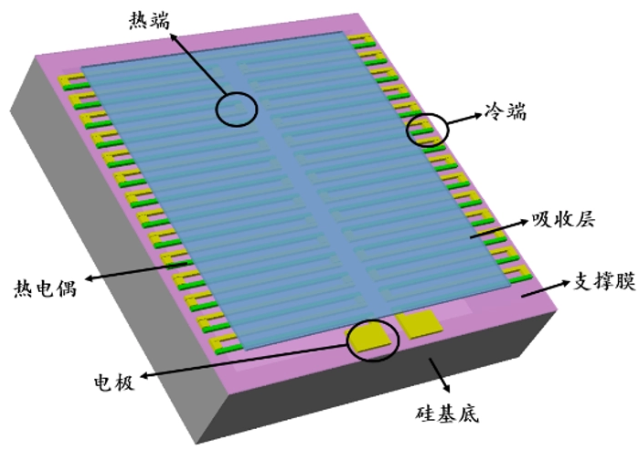
MEMS Integration: Utilizes Micro-Electro-Mechanical Systems (MEMS) technology to miniaturizetraditional thermopile structures on silicon substrates. The key involves placing the hot junction on a micromachined structure (typically a suspended membrane) designed to absorb infrared (IR) radiation, while the cold junction connects to the thermally stable silicon substrate (heat sink).
Operation:
The target object emits infrared radiation (IR).
The sensor receives radiation through an IR filter (often tuned to specific wavelengths, e.g., 5-14μm for human body radiation).
Radiation energy is efficiently absorbed and converted into heat by the absorption layer (e.g., black material or specific metal structures) in the hot junction area.
The hot junction temperature rises, creating a temperature difference (ΔT) relative to the cold junction.
This ΔT drives the series-connected thermocouples to generate a thermoelectric voltage (output voltage).
This voltage signal is processed by signal conditioning circuitry (e.g., low-noise amplifier, analog-to-digital converter - ADC) to obtain the temperature reading.
Non-Contact Temperature Measurement: Safe, hygienic, fast response – no physical contact required.
High Sensitivity: Low thermal mass of MEMS structures enables rapid heating, amplified by multiple series thermocouples for measurable output.
Ultra-Low Power Consumption: Passive sensing (no active heating/cooling), ideal for battery-powered devices (e.g., forehead thermometers, ear thermometers, wearable devices).
Miniaturized Size: Chip-scale dimensions enabled by MEMS technology, perfect for compact device integration.
High Volume Cost-Effectiveness: Leverages high-volume semiconductor batch manufacturing.
Fast Response Time: Micron-scale structures have low thermal inertia for quick detection.
Wide Dynamic Range: Measures objects from near-ambient to several hundred degrees Celsius.
Passive Sensing: Only receives IR; emits no radiation.
Uncooled IR Sensor: Simpler and more cost-effective than cooled IR detectors (e.g., cryogenic HgCdTe).
Medical Electronics: Forehead thermometers, ear thermometers, skin temperature sensors, patient monitoring devices, non-contact fever screening systems.
Consumer Electronics: Smart home (HVAC, microwaves, ovens, water heaters, dryer temperature control), smart appliances, wearable devices (health monitoring), smartphones (ambient temperature, proximity sensing).
Industrial Automation: Process monitoring, equipment condition monitoring (motor/bearing overheating), production line control, non-contact temperature sensors, industrial safety.
Automotive Electronics: Occupant detection, climate control systems, battery thermal management (EVs), entry-level night vision assistance.
Security & Surveillance: Human presence detection, intrusion alarms, thermal screening systems.
Smart Building: HVAC control, energy management, people counting.
IoT (Internet of Things): Environmental sensing nodes, smart agriculture, intelligent hardware.
The exceptional performance of thermopile MEMS sensors relies on mature semiconductor MEMS manufacturing processes.This advanced technology combines integrated circuit (IC) fabrication with micromachining to batch-produce intricate 3D microstructures on silicon wafers.
Material Selection: Primary substrate: Silicon wafers. Thermocouple materials: Polysilicon, metals, or silicides. Requires low thermal conductivity materials for thermal isolation (e.g., Silicon Dioxide - SiO₂, Silicon Nitride - Si₃N₄, Porous Silicon) and IR absorber layers.
Thin Film Deposition: Techniques like Physical Vapor Deposition (PVD) and Chemical Vapor Deposition (CVD) grow/deposit functional layers (conductors, insulators, semiconductors, sacrificial layers).
Photolithography: Uses photoresist and photomask to transfer microstructural patterns onto the wafer surface via UV exposure. Critical for defining features.
Etching:
Dry Etching: Uses plasma for anisotropic etching (high precision, e.g., Reactive Ion Etching - RIE, Deep Reactive Ion Etching - DRIE).
Wet Etching: Uses chemical solutions for isotropic/anisotropic etching. Often removes sacrificial layers.
Etching creates the desired 3D structures in films or the substrate.
Sacrificial Layer Technology: An MEMS cornerstone. A sacrificial layer material (e.g., SiO₂, photoresist) is deposited first. Structures needing suspension (like the thermopile hot membrane) are built on top. Selective etching later releases the movable microstructure by removing the sacrificial layer. Crucial for forming suspended hot junctions.
Wafer Bonding: Wafer-level bonding joins the MEMS structure wafer to an Application-Specific Integrated Circuit (ASIC) wafer containing signal processing electronics for system integration and protection.
Packaging: Protects the delicate die with hermetic sealing (e.g., TO (Transistor Outline) can packaging, ceramic packaging, wafer-level packaging - WLP), integrating the IR filter. Vital for sensor reliability against moisture, dust, and stress.
High-Volume Manufacturing (HVM): Fabricates thousands of devices per wafer, drastically reducing cost.
High Precision: Micron/sub-micron accuracy ensures performance consistency and reliability.
Miniaturization: Enables chip-scale complex microstructures.
Integration Capability: Facilitates integration with CMOS signal conditioning circuits for monolithic or wafer-level packaged smart sensor systems.
High Reliability: Based on mature semiconductor standards.
CMOS Compatibility: Many MEMS steps are compatible with standard CMOS process lines, aiding integration.
For applications demanding non-contact, cost-effective, low-power, compact, and fast-response temperature measurement, thermopile MEMS sensors are among the most practical and economical solutions available.
The underlying semiconductor MEMS fabrication provides a robust manufacturing foundation, ensuring performance, reliability, and mass production scalability.
Core: Thermopile MEMS Sensor, Semiconductor MEMS Process, MEMS, Micro-Electro-Mechanical Systems, Non-Contact Temperature Measurement, Non-Contact Sensing, IR Sensor, Infrared Radiation, Seebeck Effect, Thermoelectric Effect, Thermocouple, Hot Junction, Cold Junction, Temperature Difference (ΔT), Thermoelectric Voltage, Output Voltage, Micromachined Structure, Suspended Membrane, Silicon Substrate, Heat Sink, IR Filter, Absorption Layer, Signal Conditioning Circuit, Low-Noise Amplifier (LNA), Analog-to-Digital Converter (ADC).
Advantages: High Sensitivity, Low Power Consumption, Miniaturized Size, Low Cost, High-Volume Manufacturing, Batch Production, Fast Response Time, Wide Dynamic Range, Passive Sensor, Uncooled IR Sensor, Battery-Powered.
Applications: Medical Electronics, Forehead Thermometer, Ear Thermometer, Skin Temperature Sensor, Patient Monitoring, Non-Contact Fever Screening, Consumer Electronics, Smart Home, Smart Appliances, Wearable Devices, Smartphones, Industrial Automation, Process Monitoring, Equipment Condition Monitoring, Production Line Control, Non-Contact Temperature Sensor, Industrial Safety, Automotive Electronics, Occupant Detection, Climate Control, Battery Thermal Management, Electric Vehicles (EVs), Security, Surveillance, Human Presence Detection, Intrusion Alarm, Smart Building, HVAC, Energy Management, People Counting, IoT, Internet of Things, Environmental Monitoring, Smart Agriculture, Intelligent Hardware.
Process: Semiconductor Manufacturing, IC Fabrication, Micromachining, Silicon Wafer, Silicon Substrate, Polysilicon, Metals, Silicides, Low Thermal Conductivity, Thermal Isolation, Silicon Dioxide (SiO₂), Silicon Nitride (Si₃N₄), Porous Silicon, Thin Film Deposition, PVD, CVD, Photolithography, Photoresist, Photomask, UV Exposure, Etching, Dry Etching, Wet Etching, RIE, DRIE, Sacrificial Layer Technology, Sacrificial Layer, SiO₂ Sacrificial Layer, Release Structure, Wafer Bonding, Wafer-Level Bonding, ASIC, Packaging, Hermetic Packaging, TO Can Packaging, Ceramic Packaging, Wafer-Level Packaging (WLP), CMOS Signal Processing, Monolithic Integration, CMOS Compatibility.
Process Advantages: High-Volume Manufacturing (HVM), High Precision, Miniaturization, Integration Capability, High Reliability.
Sub 1: PlutoChip Co., Ltd -Discrete Devices and Integrated Circuits- www.plutochip.com
Sub 2: PlutoSilica Co., Ltd -Silicon Wafer and Glass Wafer Manufactory-