What Is TGV and Why Is It Gaining Attention?
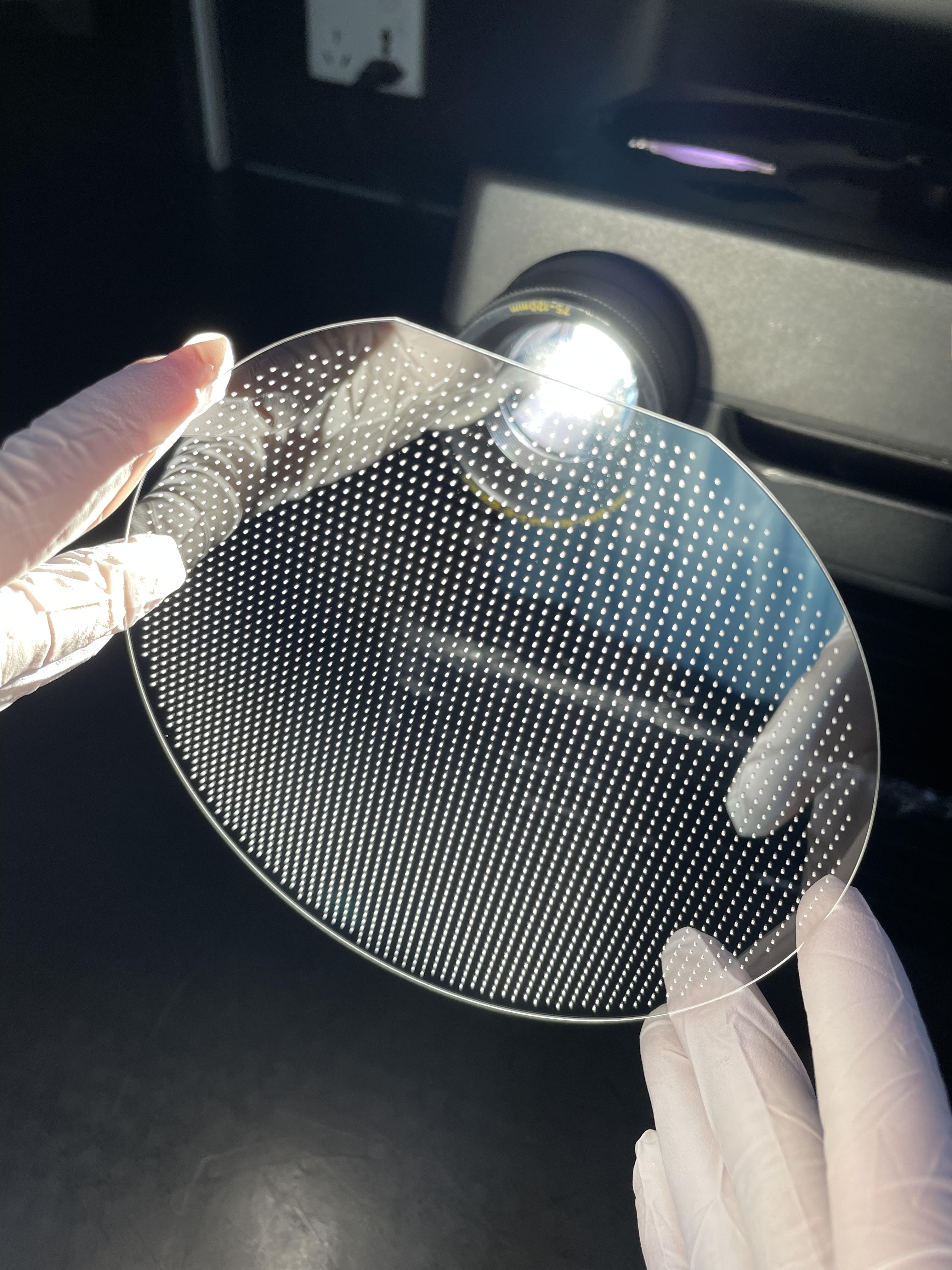
In simple terms, TGV involves fabricating micron‑sized holes through a glass wafer and filling them with metal (e.g., copper) to achieve vertical electrical interconnections between chips or wafers.
The technology addresses critical bottlenecks of the current mainstream TSV (Through Silicon Via) approach. In high‑frequency, high‑speed applications, TSV suffers from signal loss and parasitic effects due to silicon’s semiconducting nature. Additionally, the complex insulation deposition process makes TSV costly.
Core Advantages of TGV
Compared to TSV, TGV offers several compelling benefits:
Glass is an excellent insulator, with a dielectric constant only about 1/3 that of silicon, and a loss tangent 2‑3 orders of magnitude lower. This drastically reduces signal loss and interference, ensuring signal integrity – especially critical for 5G/6G communications and AI chips.
Glass substrates are far cheaper than silicon ones. Moreover, glass is intrinsically insulating, eliminating the need for depositing complex insulation layers inside the via holes, thereby simplifying the process and cutting costs. Estimates suggest that glass interposers can be produced at only 1/8 the cost of silicon interposers.
Glass has a coefficient of thermal expansion (CTE) closely matching that of silicon chips, effectively alleviating thermal stress. Even in ultra‑thin forms (<100 µm), glass wafers exhibit minimal warpage, ensuring packaging reliability.
Glass can be readily obtained in large panels exceeding 2 m × 2 m, enabling parallel processing over a large area, which further boosts production efficiency and economies of scale.
Key Manufacturing Processes for TGV
TGV fabrication is a highly precise, multi‑step engineering process:
-
Glass Substrate Preparation – High‑quality borosilicate or quartz glass is selected.
-
Via Formation (Core Technology) –
-
Laser‑Induced Deep Etching: Currently the mainstream method. Ultra‑short pulsed lasers selectively modify the glass, followed by chemical etching (e.g., with hydrofluoric acid) to remove the modified regions, creating vias. This method offers high precision, speed, and minimal damage. Advanced systems can achieve vias as small as 5 µm in diameter with aspect ratios up to 20:1.
-
Alternative methods include sandblasting, focused discharge, plasma etching, and photosensitive glass processes, but these often have limitations in control, efficiency, or cost.
-
Cleaning and Surface Treatment – Removing residues and activating via walls to enhance metal‑glass adhesion.
-
Metallization (Conductive Filling) –
-
Seed Layer Deposition: A thin metal layer (e.g., copper, titanium) is deposited on the via walls via PVD or CVD.
-
Electroplating Filling: Using the seed layer as a cathode, the vias are completely filled with copper to form conductive pillars.
Planarization and Post‑Processing – CMP removes excess surface metal, achieving a flat surface. Followed by RDL formation, testing, and dicing.
Main Application Areas
TGV technology finds use across a wide range of fields, from consumer electronics to high‑performance computing:
-
AI & High‑Performance Computing (HPC) – As glass interposers in 2.5D/3D packaging, enabling high‑density, high‑speed interconnects between logic chips and HBM (High‑Bandwidth Memory). This is currently one of the most pressing applications.
-
High‑Frequency Communications (5G/6G) – Providing low‑loss, high‑signal‑integrity packaging solutions for RF chips, millimeter‑wave radar, etc.
-
Optical Modules & CPO (Co‑Packaged Optics) – Leveraging glass’s high transparency over a broad spectrum for ideal packaging substrates in optical modules and CPO.
-
MEMS & Sensors – Used in advanced 3D packaging for high‑end MEMS and sensors.
-
Novel Displays – Potentially breaking through current packaging bottlenecks in new display technologies.
TGV technology, with its superior high‑frequency performance, cost benefits, and mechanical stability, is emerging as a key enabler for next‑generation advanced packaging. It is poised to become a mainstream interconnect solution in AI chips, 5G communications, and high‑performance computing.