| Parameters range for Silicon on Sapphire (SOS) Epi Wafers |
| Wafer diameter |
76 mm, 100 mm, 150 mm |
| Orientation |
(1012) ± 1º (R-plane) |
| Substrate dopant |
- |
| Epi-layer thickness, µm |
0,3 – 2,0 |
| Epi-layer dopant |
Phosphorous, Boron |
| Epi-layer resistivity, Ohm.cm |
|
| n-type |
according to spec. |
| p-type |
1,0 – 0,01 |
Heteroepitaxy of 5-6 silicon
With the development of large-scale and ultra large scale integrated circuits, epitaxy technology has been widely used. In addition to the homogeneous epitaxy of silicon on silicon substrate, the "SOS" epitaxy growth of silicon on sapphire and spinel substrate and the "SOI" heteroepitaxy growth of silicon on insulating substrate have also been developed. These two technologies and SiGe / I are briefly introduced in this section
5-6-1 SOS Technology
SOS is the abbreviation of "Silicon on sapphire" and "Silicon on spinel", i.e. epitaxial growth of silicon on sapphire or spinel substrate.
Sapphire (a-Al2O3) and spinel (MgO · Al2O3) are good insulators. Using them as substrates to epitaxial grow silicon to make integrated circuits can eliminate the interaction between components of integrated circuits, not only reduce leakage current and parasitic capacitance, enhance radiation resistance and reduce power consumption, but also improve integration and realize double-layer wiring. They are ideal materials for large-scale and super large-scale integrated circuits 。
1. Selection of substrate materials
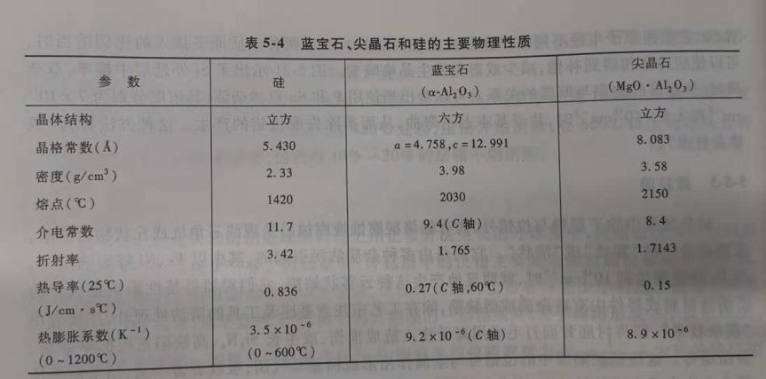
When choosing heteroepitaxial substrate materials, the first consideration is the compatibility between the epitaxial layer and substrate materials. Among them, crystal structure, melting point, vapor pressure, coefficient of thermal expansion and so on have a great influence on the quality of epitaxial layer. Secondly, the contamination of substrate on the epitaxial layer must be considered. At present, sapphire and spinel are the most suitable materials for silicon epitaxy. Table 5-4 lists the main physical properties of the two materials and silicon for comparison.
In terms of crystal structure, sapphire is hexagonal system, spinel is cubic system, and three silicon cells are consistent with two spinel cells. The mismatch of the two cells along (100 direction) is 0.7%. However, the spinel prepared by flame method is mostly aluminum rich. The lattice constant of this kind of spinel decreases with the increase of Al2O3 content, resulting in the increase of mismatch. On the other hand, the similar thermal expansion coefficient between the substrate and the epitaxial layer is one of the important factors for obtaining excellent heteroepitaxial layer. If the difference is large, the larger stress will be produced near the interface when the temperature changes, which will increase the defects of epitaxial layer, even warping, thus affecting the performance and thermal stability of materials and devices.
Considering lattice matching, thermal matching, reducing self doping and capacitance effect, spinel is a better substrate material than sapphire. However, the properties of silicon epitaxial layer on spinel are strongly dependent on the substrate components, which vary with different preparation methods and processing conditions. Therefore, although the silicon epitaxial layer on spinel substrate is superior to that on sapphire substrate, sapphire is widely used as silicon epitaxial substrate in current industrial production due to its poor reproducibility, high thermal conductivity and mature preparation process.
2. OS epitaxial growth
The equipment and basic process of OS epitaxial growth are the same as that of general silicon Homoepitaxy. The cutting, grinding, polishing and cleaning of substrate are basically the same, except that sapphire is harder than silicon, and the grinding and polishing time is longer.
In the process of SOS epitaxial growth, it is worth noting that the self doping effect is more serious, because under the condition of epitaxial growth, the substrate surface will react as follows:
Al2O3(s)+2HCl(g)+2H2(g)=2A1Cl(g)↑+3H20(g)
The chlorides of low valent aluminum are gaseous, which corrode the substrate and cause defects in the epitaxial layer. In addition, H2 and deposited silicon also corrode the substrate, and the reaction is as follows:
2H2(g)+al2O3(s)=al20(g)↑+2H2(g)
5Si(s)+2al2O3(s)=al20(g)↑+5Si(g)↑+2Al(s)
Before the substrate surface is completely covered by Si (at least the epitaxial layer is 10 ~ 20nm), all the above corrosion reactions are in progress. After the substrate surface is covered, these corrosion reactions will occur on the back of the substrate. Cause contamination such as a1o. In addition, due to the corrosion of the substrate surface, defects in the epitaxial layer will be increased, and even local polycrystalline growth will occur. Because the corrosion of SiCl4 to substrate is greater than that of SiH4, it is more advantageous to use SiH4 thermal decomposition method for SOS epitaxial growth.
In order to solve the contradiction between growth and corrosion, epitaxial growth methods such as double rate growth and two-step epitaxial growth can be used. The double rate growth method uses high growth rate (1 ~ 2 μ M / Mn) to quickly cover the substrate surface (growth 100 ~ 200nm). Then, it grows to the required thickness at a low growth rate (about 0.3m / min).
The two-step epitaxy is a comprehensive utilization of the advantages of SiH4 / H2 and sicl4h2 systems. In the first step, SiH4 / H2 system was used to rapidly cover the substrate surface, and then SiCl4 / 2 system was used to grow to the required thickness.
Due to the mechanical damage of the substrate surface and the corrosion between the growth components and the substrate, lattice mismatch, improper valence bond, strain effect and other factors, it is inevitable to introduce high-density dislocation, twin, intergranular boundary and other lattice defects in the epitaxial layer of SOS. These defects interact with heavy metal impurities such as Cu, Fe and form a series of deep energy levels in the forbidden band. In addition, there are some crystal defects in the epitaxial layer, such as A1 local precipitation and its oxide. They act as recombination, scattering and capture centers, which make the carrier concentration, mobility and minority carrier lifetime decrease. Therefore, the quality of SOS epitaxial layer can not catch up with that of homogeneous epitaxial layer, and the thinner the epitaxial layer, the worse the performance. In the future, it is an important subject for the development of SOS technology to improve the crystal integrity of SOS epitaxial layer, reduce self doping, make its performance close to the level of homogeneous silicon epitaxial layer and have good thermal stability.