中文 | En
Products
Position: Home > Products > Products > Silicon Wafer
Silicon Wafer
MEMS Wafer
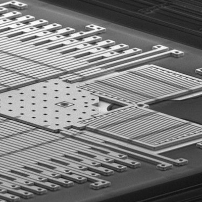
Wafer solutions for leading-edge technology development MEMS components are used in a wide variety of systems ranging from low volume sensoric elements in harsh industrial environments to high volume consumer goods. MEMS is forecasted to impact almost every product category bringing together silicon based microelectronics and micromachining technology in the same package or on the same chip.
Product Detail
 
  Czochralski Float Zone Float Zone
Diameter 100-150 mm 50-150 mm* 100-150 mm*
Crystal orientation <100> <111> <100> <111> <100> <111>
Orientation accuracy <0.5° <0.5° <0.5°
Type and dopant Undoped, n-type,
p-type
Undoped, n-type,
p-type
Undoped, n-type,
p-type
Dopant As, B, P, and Sb P, B P, B
Bulk resistivity 0.001-60 1-30,000 1-30,000
Bulk lifetime >20 µs >1,000 µs >1,000 µs
Wafer thickness 200-1,500 µm 200-1,500 µm 200-1,500 µm
Wafer thickness
tolerance
±15 µm ±15 µm ±5 µm
TTV <5 µm or <9 µm <5 µm or <9 µm <2.5 µm
TIR <3 µm <3 µm <1 µm
Wafer surface finish Single side polished,
Double side polished
Single side
polished
Double side
polished

       
Wafer solutions for leading-edge technology development MEMS components are used in a wide variety of systems ranging from low volume sensoric elements in harsh industrial environments to high volume consumer goods. MEMS is forecasted to impact almost every product category bringing together silicon based microelectronics and micromachining technology in the same package or on the same chip.
 
MEMS components require superior mechanical properties of the base silicon material. Pluto fulfills these requirements from all part of the electronics industry grounded on more than half a
century’s experience in manufacturing premium quality silicon wafers. The manufacture is based on Float Zone and Czochralski technology, respectively.
 
Pluto has specialised in growing Float Zone crystals with superior control of dopant content and distribution and with very low levels of contaminants. This is especially beneficial for applications requiring very low concentrations of oxygen such as power MEMS components, high efficiency microstructured solar cells and photodiodes as well as RF MEMS devices on high resistivity silicon.
 
To complete the range of MEMS products, Topsil also offers Czochralski wafers. Czochralski wafers are traditionally being used in MEMS applications with focus on the mechanical parameters and not on the bulk properties of the silicon. Most applications require low oxygen content, but a limit of 18 ppma (new ASTM) is sufficient in many cases.

 
Sub 1: PlutoChip Co., Ltd    -Discrete Devices and Integrated Circuits-    www.plutochip.com
Sub 2: PlutoSilica Co., Ltd   -Silicon Wafer and Glass Wafer Manufactory-
Copyright © 2020 | PlutoSemi Co., Ltd | All Rights Reserved