| Diameter |
2" |
3" |
4" |
5" |
6" |
8" |
12" |
| Grade |
Prime Test Dummy |
| Growth Method |
CZ |
| Orientation |
< 1-0-0 > , < 1-1-1 > , < 1-1-0 > |
| Type/Dopant |
P Type/Boron , N Type/Phos, N Type/As, N Type/Sb |
| Thickness (um) |
279 |
380 |
525 |
625 |
675 |
725 |
775 |
| Thickness Tolerance |
Standard ± 25μm, Maximum Capabilities ± 5μm |
± 20μm |
± 20μm |
| Resistivity |
0.001 - 100 ohm-cm |
| Surface Finished |
P/E , P/P, E/E, G/G |
| TTV (um) |
Standard < 10 um, Maximum Capabilities <5 um |
| Bow/Warp (um) |
Standard <40 um, Maximum Capabilities <20 um |
<40μm |
<40μm |
| Particle |
<10@0.5um; <10@0.3um; <10@0.2um; |
What is silicon? What is monocrystalline silicon?
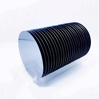
Silicon wafer: the sheet structure of single silicon material, with relatively thin thickness. There are mainly two kinds of structures, circular and square, including single crystal and polycrystalline. Single crystal is a kind of crystal material with fixed crystal orientation, which is generally used as the substrate of semiconductor integrated circuit and also used to make solar cell. Polycrystalline is a kind of crystal material without uniform fixed crystal orientation, which is generally used for solar photovoltaic power generation, or for the raw material of monocrystalline silicon. Monocrystalline silicon is a kind of excellent high-purity semiconductor material. The purity of IC level is required to be more than 9N (99.999999%), and even 11n (99.9999999%) for zone melting monocrystalline silicon wafer. Generally, CZ and FZ are used to form long crystals, whose orientation is determined by seed crystal. Monocrystalline silicon is the most important semiconductor material, accounting for more than 90% of the semiconductor material market, which is the basic material of information technology and integrated circuit. The production of silicon wafer usually has the following steps:
1) long crystal, which can be divided into CZ and FZ, because the fused polycrystalline material will directly contact with the quartz crucible, so the impurities in the quartz crucible will contaminate the fused polycrystalline. The CZ method is suitable for drawing large-diameter (300 mm) silicon wafers, which is the main semiconductor silicon wafer material at present. As the polycrystalline raw materials are not in contact with the quartz crucible, there are few internal defects and low carbon and oxygen content, but the price is expensive and the cost is high. It is suitable for high-power devices and some high-end products.
2) slicing and drawing of the single crystal silicon rod need to cut off the head and tail material, then roll and grind it to the required diameter, cut the flat edge or V groove, and then cut into thin silicon wafer. At present, diamond wire cutting technology is usually used, with high efficiency and good warpage and curvature of silicon wafer. A small number of special shaped pieces can be cut with an inner circle.
3) grinding: after slicing, the damaged layer on the cutting surface needs to be removed by grinding to ensure the quality of the silicon wafer surface, about 50um.
4) corrosion: corrosion is to further remove the damaged layer caused by cutting and grinding, so as to prepare for the following polishing process. Corrosion usually includes alkali corrosion and acid corrosion. At present, due to environmental factors, most of them adopt alkali corrosion. The removal amount of corrosion can reach 30-40um, and the surface roughness can also reach micron level.
5) polishing: polishing is an important process for silicon wafer production. Polishing is to further improve the surface quality of silicon wafer through CMP (chemical mechanical polished) technology, so that it can meet the requirements of chip production. After polishing, the surface roughness is usually RA < 5A.
6) cleaning and packaging: as the linewidth of the integrated circuit is getting smaller and smaller, the requirements for improving the particle size index are getting higher and higher. Cleaning and packaging is also an important process for silicon wafer production. Most particles attached to the surface of silicon wafer > 0.3um can be cleaned by megasonic cleaning, and then the silicon wafer surface can be made by vacuum sealing packaging or inert gas packaging with a plug box free of cleaning The surface cleanliness meets the requirements of IC.