| Diameter |
2" |
3" |
4" |
5" |
6" |
8" |
12" |
| Grade |
Prime |
| Growth Method |
FZ (Flow Zone) |
| Orientation |
< 1-0-0 > , < 1-1-1 > , < 1-1-0 > |
| Type/Dopant |
Intrinsic, Undoped, P Type/Boron , N Type/Phos, NTD, Gas-Doped, |
| |
|
|
|
|
|
|
|
| Resistivity |
>5,000 Ω•cm, >10,000 Ω•cm, >20,000 Ω•cm |
| Life Time |
>500us, >1,000us, |
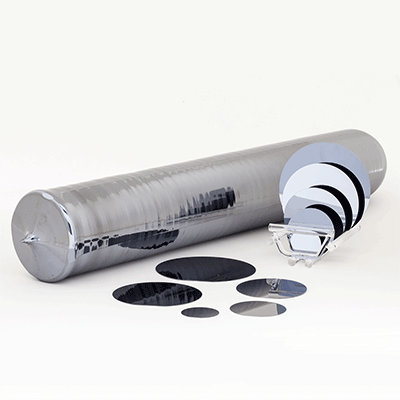
Float Zone Ingot
Float Zone ( also Floating Zone or FZ ) wafers are used primarily for applications in which very high resistivity or the absence of oxygen are necessary for good device performance. Such applications include discrete power, MOS power, high efficiency solar cells and RF/wireless communication chips.
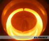
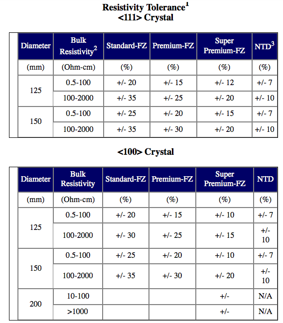
FZ wafers are sliced from ingots manufactured by the float zone process, in which a polycrystalline or monocrystalline silicon rod is passed through a zone refining apparatus which melts and then re-solidifies the silicon into a mono-crystalline rod. During the zone refining process, all impurities including substitutional dopants such as boron, phosphorus, arsenic, antimony and metallic impurities are pushed ahead of the melt region and reincorporated into the mono-crystalline ingot at much lower concentrations. This permits very low doping levels and very high resistivities and the elimination of oxygen.
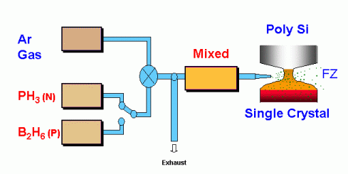
FZ ingots can be intentionally doped through the introduction of gas dopants at the melt interface, or doped later through the Neutron Transmutation Doping (NTD) process in which silicon isotopes Silicon30 are converted in Phosphorous31 leading to an n-type material.
PLUTO offers both gas-doped and NTD FZ wafers, as well as high resistivity undoped FZ. Diameters up to 200mm.
PLUTO also offers SOI wafers built with FZ used for the bond and base wafers. These SOI wafers are seeing growing demand for RF/wireless applications.